Display panel and display device
A technology of display panel and electrode plate, applied in the direction of instruments, semiconductor devices, electrical components, etc., can solve the problems of large wiring space, different capacitance, uneven transmission signal, etc., to increase the compensation ability, improve the uniformity, and increase the compensation ability Effect
- Summary
- Abstract
- Description
- Claims
- Application Information
AI Technical Summary
Problems solved by technology
Method used
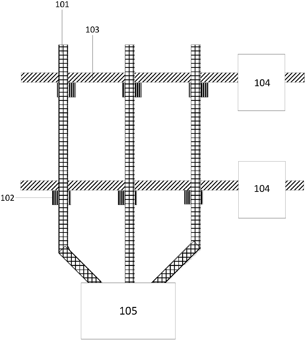
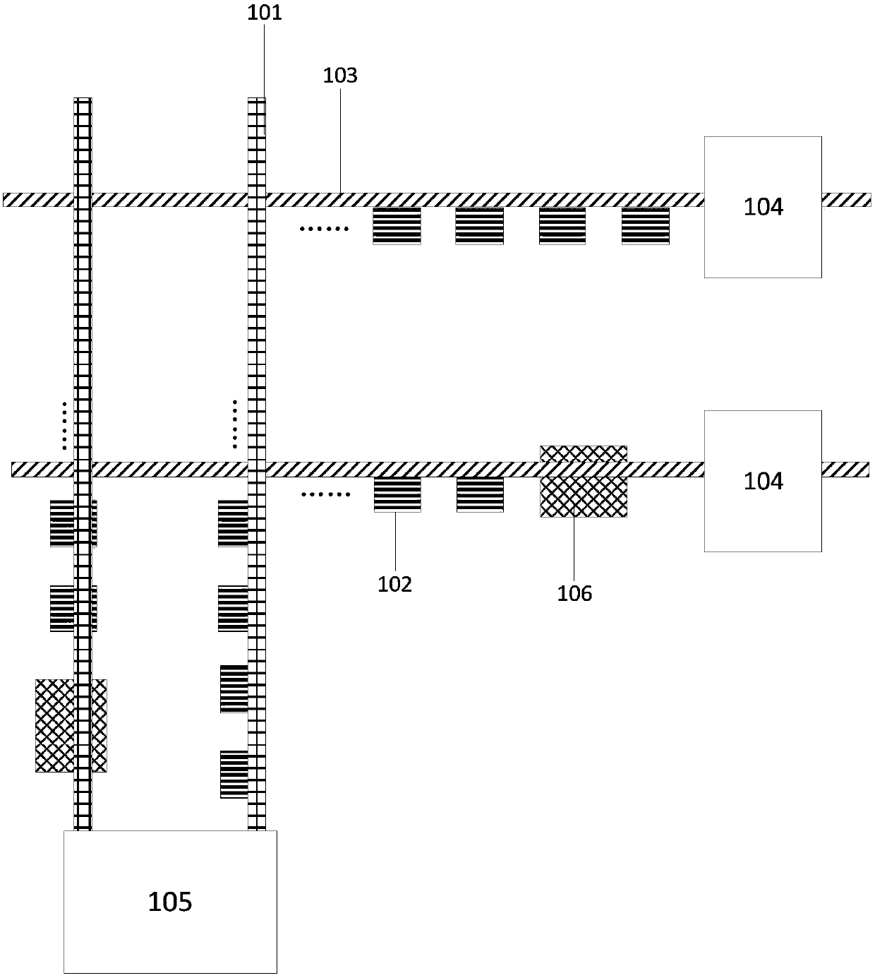
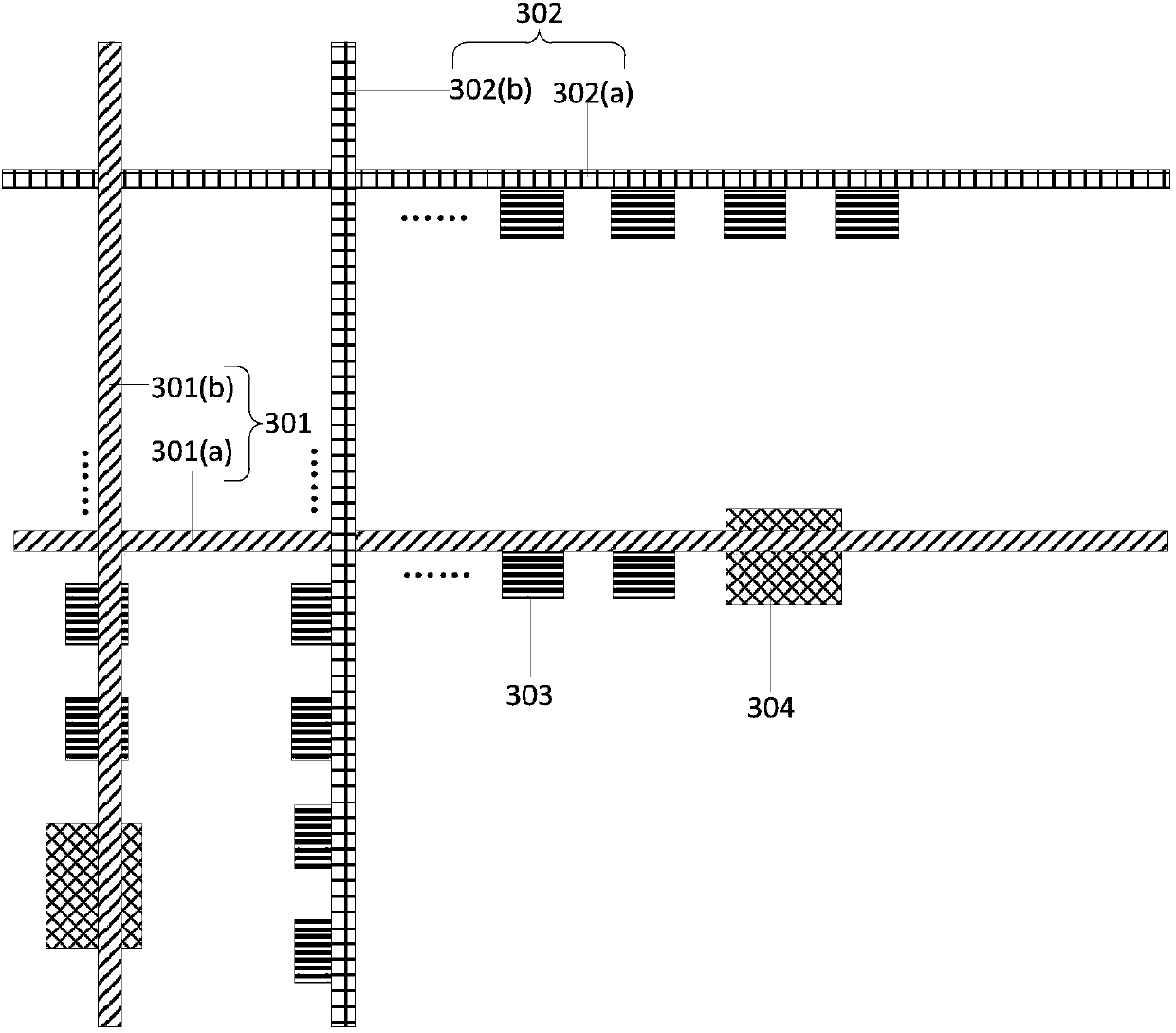
Image

Examples
Embodiment 1
[0088] Such as Figure 5 As shown, the compensation capacitor includes a first plate 011 , a second plate 012 and a third plate 013 .
[0089] Wherein, the first electrode plate 011 and the gate metal layer 001 are arranged on the same layer, and can be fabricated in the same process using the same material;
[0090] The second pole plate 012 is set on the same layer as the second metal pole plate 002, and can be fabricated in the same process using the same material;
[0091] The third electrode plate 013 and the source-drain metal layer 003 are arranged in the same layer, and can be fabricated in the same process using the same material.
[0092] Wherein, the first pole plate 011 and the third pole plate 013 are located on both sides of the second pole plate 012, and the first pole plate 011 and the third pole plate 013 are arranged on the IMD The via holes in the layer 504 and the ILD layer 505 are electrically connected, and the orthographic projection of the second plat...
Embodiment 2
[0094] Such as Image 6 As shown, the compensation capacitor includes a first plate 011, a second plate 012, a third plate 013 and a fourth plate 014; wherein,
[0095] The first electrode plate 011 and the gate metal layer 001 are arranged in the same layer, and can be fabricated in the same process using the same material;
[0096] The second pole plate 012 is set on the same layer as the second metal pole plate 002, and can be fabricated in the same process using the same material;
[0097] The third electrode plate 013 is set on the same layer as the source-drain metal layer 003, and can be fabricated in the same process using the same material;
[0098] The fourth electrode plate 014 is disposed on the same layer as the active layer 004, and can be manufactured using the same material in the same process.
[0099] Wherein, the first pole plate 011 and the third pole plate 013 are located on both sides of the second pole plate 012, and the first pole plate 011 and the th...
Embodiment 3
[0101] Such as Figure 7 As shown, the compensation capacitor includes a first plate 011, a second plate 012, a third plate 013, a fourth plate 014 and a fifth plate 015; wherein,
[0102] The first electrode plate 011 and the gate metal layer 001 are arranged in the same layer, and can be fabricated in the same process using the same material;
[0103] The second pole plate 012 is set on the same layer as the second metal pole plate 002, and can be fabricated in the same process using the same material;
[0104] The third electrode plate 013 is set on the same layer as the source-drain metal layer 003, and can be fabricated in the same process using the same material;
[0105] The fourth pole plate 014 and the active layer 004 are arranged on the same layer, and can be fabricated in the same process using the same material;
[0106] The fifth electrode plate 015 is disposed on the same layer as the pixel electrode layer 507, and can be manufactured using the same material i...
PUM
 Abstract
Description
Claims
Application Information
 - Generate Ideas
- Intellectual Property
- Life Sciences
- Materials
- Tech Scout
- Unparalleled Data Quality
- Higher Quality Content
- 60% Fewer Hallucinations
Browse by: Latest US Patents, China's latest patents, Technical Efficacy Thesaurus, Application Domain, Technology Topic, Popular Technical Reports.
© 2025 PatSnap. All rights reserved.Legal|Privacy policy|Modern Slavery Act Transparency Statement|Sitemap|About US| Contact US: help@patsnap.com