A vertical double-diffused metal-oxide-semiconductor field-effect transistor with a stepped high-k dielectric layer and a wide bandgap semiconductor

An oxide semiconductor and vertical double-diffusion technology, which is applied in semiconductor devices, semiconductor/solid-state device manufacturing, transistors, etc., can solve problems such as no advantages

Active Publication Date: 2020-05-01
XIDIAN UNIV
View PDF7 Cites 0 Cited by
  • Summary
  • Abstract
  • Description
  • Claims
  • Application Information

AI Technical Summary

Problems solved by technology

Therefore, the program does not currently reflect the advantages of

Method used


Image

  • A vertical double-diffused metal-oxide-semiconductor field-effect transistor with a stepped high-k dielectric layer and a wide bandgap semiconductor

Examples


Embodiment Construction

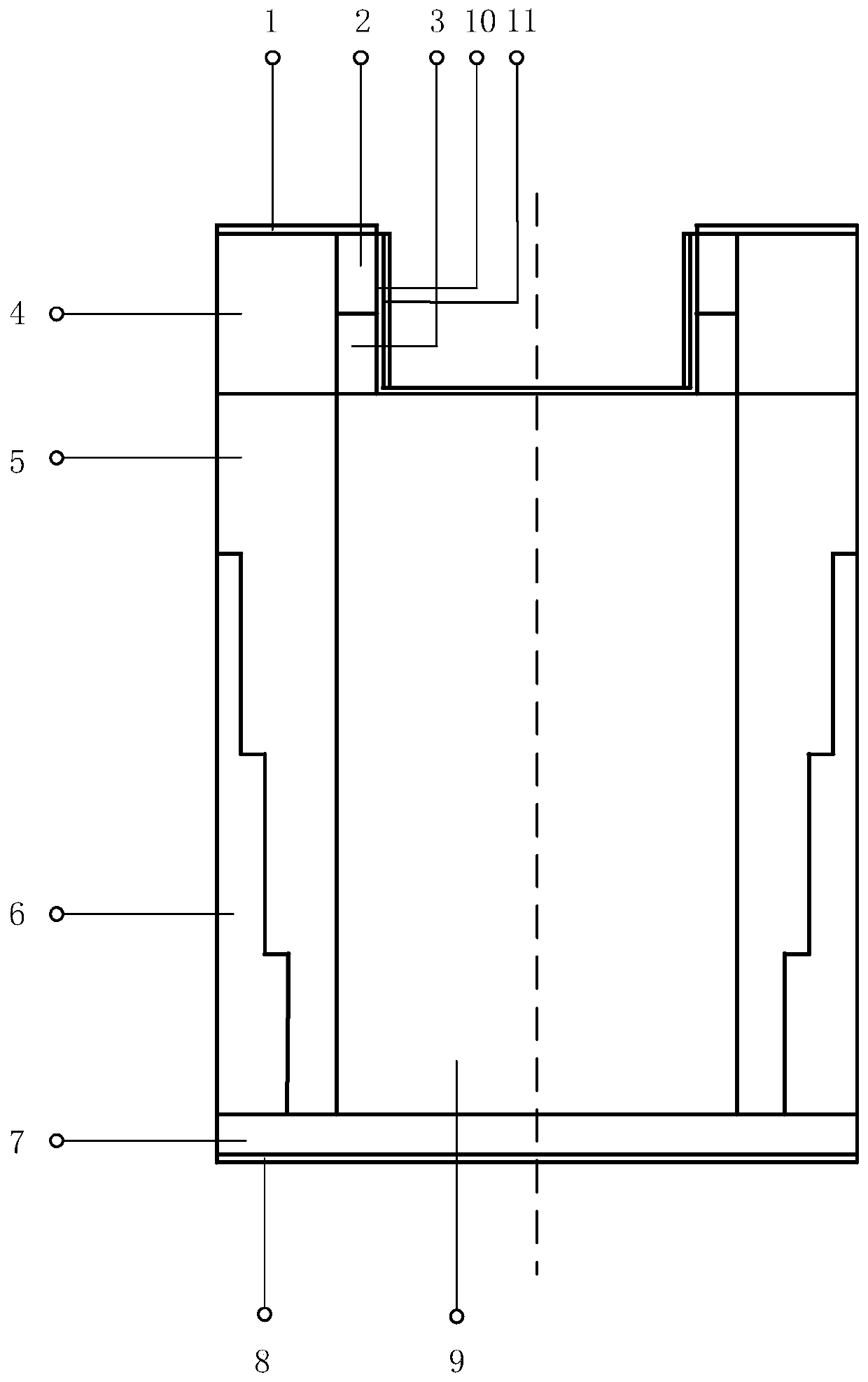
[0046] Such as figure 1 As shown, the longitudinal double-diffused metal oxide semiconductor field effect transistor with a stepped high-K dielectric layer includes:

[0047] The wide bandgap semiconductor material substrate 7 serves as the drain region at the same time, and the doping concentration is the concentration of common materials, with a typical value of 1×10 13 cm -3 ~1×10 15 cm -3 ; Typical representatives of wide bandgap semiconductor materials are third-generation semiconductor materials such as gallium nitride, silicon carbide or diamond;

[0048] The drift region 9 formed by the epitaxial layer on the substrate; the depth (length) of the drift region is determined according to the breakdown voltage requirements of the device, for example, when the withstand voltage is 600V, a 25-50 μm wide bandgap semiconductor is epitaxially grown on the substrate The material forms a drift zone;

[0049] a base region 3 formed by doping on the drift region;

[0050] A t...


PUM

PropertyMeasurementUnit
relative permittivityaaaaaaaaaa

Abstract

The invention provides a stair high K dielectric layer broad-band gap semiconductor vertical dual-diffused metal oxide semiconductor field effect transistor (VDMOS); a stair high dielectric constant (high K) dielectric layer is formed on two sides of a device drift region; a low dielectric constant dielectric layer is arranged below the High K dielectric layer stair; when the device is shut down,the High K dielectric layer assist an exhaust drift region through the electric field modulation, thus greatly improving the exhaust capability of the device drift region, increasing the device driftregion doped concentration, and reducing the conduction resistance; the subarea optimized stair High K dielectric layer can import a new electric field peak into the drift region, thus further optimizing the drift region field distribution; with said advantages combined, the device is higher in voltage withstand and lower in conduction loss under the same drift region length conditions.

Description

technical field [0001] The invention relates to the field of semiconductor devices, in particular to a trench (Trench) type vertical double-diffused metal oxide semiconductor field effect transistor. Background technique [0002] Wide bandgap semiconductor materials have the characteristics of large band gap, high critical breakdown electric field, high thermal conductivity and high electron saturation drift velocity, so they have very broad application prospects in the field of high-power, high-temperature and high-frequency power electronics. At present, among the field effect transistors based on SiC, a typical wide-bandgap semiconductor, the vertical double-diffused metal-oxide-semiconductor field effect transistor (VDMOS) is one of the widely studied objects. In 1991, Professor Chen Xingbi independently proposed the composite buffer layer (Composite Buffer, CB) structure, that is, the super-junction withstand voltage layer, which successfully broke the "silicon limit" o...

Claims


Application Information

Patent Timeline
Patent Type & Authority Patents(China)
IPC IPC(8): H01L29/78H01L21/336
CPCH01L29/66045H01L29/66068H01L29/66522H01L29/66712H01L29/7802
Inventor 段宝兴谢丰耘赵逸涵曹震杨银堂
Owner XIDIAN UNIV
Why Eureka
Try Eureka