GaN-based p-GaN enhanced HEMT device and manufacturing method thereof

An enhancement-mode, p-gan technology, applied in semiconductor/solid-state device manufacturing, semiconductor devices, electrical components, etc., can solve the problems of p-GaN difficulty, device threshold instability, low activation rate, etc., to achieve cap layer thickness and Reduced doping concentration requirements, low doping concentration and thickness requirements, and improved depletion effect

Inactive Publication Date: 2019-06-14
SUZHOU INST OF NANO TECH & NANO BIONICS CHINESE ACEDEMY OF SCI
View PDF4 Cites 0 Cited by
  • Summary
  • Abstract
  • Description
  • Claims
  • Application Information

AI Technical Summary

Problems solved by technology

For example, to realize the enhanced type of concave gate technology, it is necessary to remove part of the barrier layer under the gate to reduce the concentration of two-dimensional electron gas in the channel under the gate to achieve the enhanced effect. The disadvantage is that the etching accuracy is too high. And etching can easily lead to changes in the interface, introduce interface states, and affect the performance of the device
F ion implantation under the gate uses F ions to deplete the two-dimensional electron gas under the gate. The disadvantage lies in the instability of F ion implantation, which leads to unstable threshold of the device.
Cascode cascade is a method of cascading depletion-mode devices and Si devices to achieve enhanced mode. The disadvantage is that it increases energy consumption and is limited by the performance requirements of Si devices.
The method of the p-GaN cap layer is to control the two-dimensional electron gas in the channel by means of polarization, but limited by the low activation rate, it is difficult to realize p-GaN with high doping concentration, so it is necessary to realize the p -GaN cap layer is thicker, which leads to reduced gate drive capability

Method used


Image

  • GaN-based p-GaN enhanced HEMT device and manufacturing method thereof
  • GaN-based p-GaN enhanced HEMT device and manufacturing method thereof
  • GaN-based p-GaN enhanced HEMT device and manufacturing method thereof

Examples


Embodiment 1

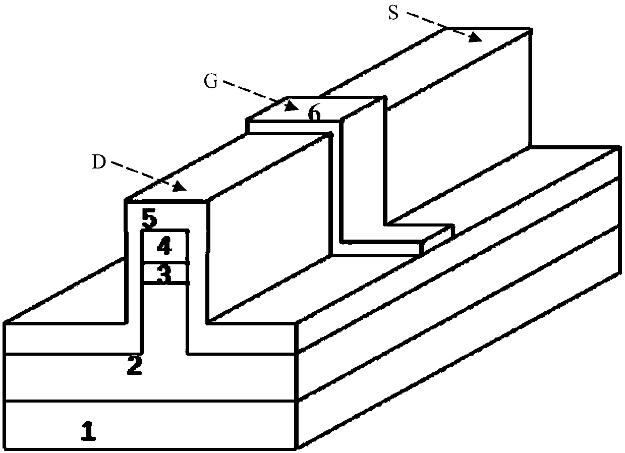
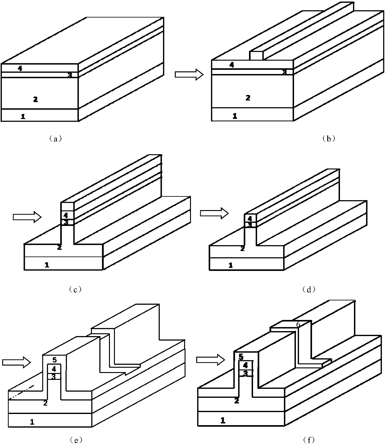
[0127] Embodiment 1: Fabricate a p-GaN / AlGaN / GaN enhanced HEMT device on a Si substrate.

[0128] Step 1: growing a buffer layer.

[0129] A low-temperature AlN buffer layer and a GaN buffer layer were grown on a Si substrate by MOCVD, wherein the AlN low-temperature growth temperature was 700° C., the thicknesses were 20 nm, and the thickness of the GaN buffer layer was 2 μm.

[0130] Step 2: growing a GaN channel layer and a barrier layer.

[0131] GaN channel layer and AlGaN barrier layer are epitaxially grown on the buffer layer by MOCVD, the thicknesses are 5nm and 20nm respectively, forming the following figure 2 The device structure shown in (a).

[0132] Step 3: growing a mask layer resistant to Cl-based etching.

[0133] 50nm thick Si grown by LPCVD 3 N 4 , Si 3 N 4 The Cl-based etching resistance can be used as a mask layer for etching to form a tunnel structure.

[0134] Step 4: Photolithographic graphics.

[0135] Using a contact photolithography machine,...


PUM

PropertyMeasurementUnit
Doping concentrationaaaaaaaaaa
Thicknessaaaaaaaaaa
Thicknessaaaaaaaaaa

Abstract

The invention discloses a GaN-based p-GaN enhanced HEMT device and a manufacturing method thereof. The device comprises a tunnel structure, a cap layer, a source, a drain and a gate, wherein the tunnel structure comprises a heterojunction; the heterojunction comprises a channel layer and a barrier layer, and two-dimensional electron gas is formed in the heterojunction; the cap layer at least formsthree-dimensional coating on the local region of the tunnel structure, and is at least used for exhausting the two-dimensional electron gas distributed in the heterojunction in the gate lower region;the source and the drain are arranged at the two ends of the tunnel structure respectively; and the gate is used for forming three-dimensional coating on the cap layer. The HEMT device has the advantages of being high in threshold voltage, and low in p-GaN cap layer doping concentration and thickness requirement and the like.

Description

technical field [0001] The invention relates to a HEMT device, in particular to a GaN-based p-GaN enhanced HEMT device and a manufacturing method thereof, belonging to the technical field of semiconductor devices. Background technique [0002] As the third-generation semiconductor material, GaN material has the characteristics of wider band gap, higher mobility, and larger breakdown electric field. It has significant advantages in power devices, microwave devices, radio frequency devices and other application fields. Due to the spontaneous polarization effect of the material itself and the piezoelectric polarization effect of the lattice difference between materials, a two-dimensional electron gas with high concentration and high mobility is naturally formed at the interface of the AlGaN / GaN heterojunction. The existence of two-dimensional electron gas greatly improves the carrier mobility, which can reduce the on-resistance, reduce the response time of the device, and impro...

Claims


Application Information

Patent Timeline
IPC IPC(8): H01L29/778H01L29/06H01L21/335
Inventor 赵杰付凯宋亮郝荣晖陈扶于国浩蔡勇张宝顺
Owner SUZHOU INST OF NANO TECH & NANO BIONICS CHINESE ACEDEMY OF SCI
Why Eureka
Try Eureka