Method for Growing III-V Epitaxial Layers and Semiconductor Structure

a technology of epitaxial layers and semiconductors, applied in the direction of semiconductor devices, basic electric elements, electrical appliances, etc., can solve the problems of low contact resistance of ohmic contacts, inability to turn transistors off, and inability to supply negative polarity gate supplies, etc., to achieve the effect of improving ohmic contacts and without jeopardizing functionality and advantages

Active Publication Date: 2014-06-12
EPIGAN NV
View PDF9 Cites 43 Cited by
  • Summary
  • Abstract
  • Description
  • Claims
  • Application Information

AI Technical Summary

Benefits of technology

[0024]The present invention therefore relates to an alternative method of growing III-V epitaxial layers on a substrate, to a semiconductor structure, to a device comprising the semiconductor structure, and to an electronic circuit comprising the device and / or the semiconductor structure. Embodiments of the present invention can have the advantage of overcoming one or more of the above disadvantages, without jeopardizing functionality and advantages thereof. An independent aspect of the present invention is a method to improve ohmic contacts to source and drain, by using a regrowth, selectively in the source and drain areas and making metallic ohmic contacts.
[0033]In the present invention in an example a method for manufacturing a transistor, such as a JFET is provided, with selectively re-grown p-type AlGaN in a gate area, using a novel in-situ deposited protection layer stack as mask. A better interface is obtained to the regrown p-type AlGaN. The protection layer stack serves as an in-situ passivation layer for the device, allows precise control of its etching in the gate area and is an excellent mask for selective epitaxial re-growth. The transistor, such as the JFET, has superior performance compared to other types of e-mode HEMTs e.g. because of its excellent passivation, suitably high threshold voltage and large gate over-drive capability.
[0043]Thereby the present invention provides a solution to one or more of the above mentioned problems. Especially a leakage current is significantly reduced, dielectric breakdown is prevented, and / or reliability of the gate is improved, and / or a well controllable process is provided, and / or the 2DEG layer does not deplete in the extrinsic device area, and / or plasma damage is prevented, and / or oxidation of a barrier top surface is prevented, and / or dispersion is prevented and / or good dynamic performance of e.g. a transistor is maintained. Any, a combination of, or all of the above mentioned disadvantages are overcome hereby, or at least (effects thereof are) significantly reduced. Advantages of the present description are detailed throughout the description.DETAILED DESCRIPTION OF THE INVENTION
[0063]It is observed that to some extent the above dimensions depend on a technology used, i.e. a more advanced technology using relatively smaller features will function better when using relatively smaller isolations and spaces.
[0067]The one or more protective layers protect the underlying active layer during subsequent processing. As a consequence the present semiconductor structure is fully compatible with other processes, in particular CMOS processes. Even further, as the active layer is protected it remains in excellent shape and can be processed further without extra precautions. Even further, by the nature of the present process, wherein the one or more protective layers are removed, such as by wet and / or dry etching, the surface of an active layer obtained thereby is in excellent condition to be further processed, such as for re-growth. The above makes clever use of advantages obtained by the present process.
[0095]The present semiconductor structure provides any, a combination of, or all of the following advantages: a leakage current that is significantly reduced, a gate dielectric breakdown that is postponed, a reliability of the gate that is improved, a suitably positive threshold voltage, a 2DEG layer that does not deplete in the extrinsic device area, no oxidation of a barrier top surface, no dispersion resulting in good dynamic performance of e.g. a transistor is maintained, etc.

Problems solved by technology

These transistors work in depletion-mode operation which means the channel has to be depleted to turn the transistor off.
For certain applications, such as e.g. power switching or integrated logic, negative polarity gate supply is undesired.
Another issue with AlGaN / GaN HEMT's is the relative high contact resistance of the ohmic contacts, because of the high bandgap of the III-nitride material and the absence of impurity doping.
This is very detrimental for the passivation of the surface of AlGaN / GaN HEMT.
The etching process to remove the p-GaN in the extrinsic device area is non-selective to the underlying layers and as such is very difficult to control.
As a consequence, etch depth is hard to control, plasma damage may result from it and the uncovered surface may be hard to passivate in further processing steps.
However, for practical applications, the threshold voltage is too low.
However, for practical applications, the threshold voltage is too low.These HEMTs are grown directly onto a substrate.
Due to the non-selective nature of the etch, the process is hard to control.
Fluorine plasma is known to have a detrimental effect on the dynamic behavior of the HEMT as it causes substantial increases in the dynamic on resistance.
Without the thermal oxidation, due to the Schottky nature of the gate, the performance of the first approach is limited by the gate over-drive (Vg<2V).
In the case of the oxidation of the Al-rich barrier, issues remain with the leakage current, dielectric breakdown and reliability of the gate oxide.
In both cases, the threshold voltage is too low for practical applications.
At zero gate bias the device channel is depleted due to the high built-in potential of the gate-channel junction.
However, SiOx is not a suitable passivation layer for HEMT devices and may cause the oxidation of the AlGaN barrier top surface, which leads to an increased dynamic on-resistance.
Furthermore, it can only be deposited ex-situ i.e. after the wafer has been removed from the epitaxial reactor and exposed to atmosphere.
Even further, as the AlGaN barrier has been exposed to atmospheric conditions as well as a number of processing steps, the passivation process may be difficult to control.
Still, above mentioned method does not seem to enable better regrowth.

Method used


Image

  • Method for Growing III-V Epitaxial Layers and Semiconductor Structure
  • Method for Growing III-V Epitaxial Layers and Semiconductor Structure
  • Method for Growing III-V Epitaxial Layers and Semiconductor Structure

Examples


Embodiment Construction

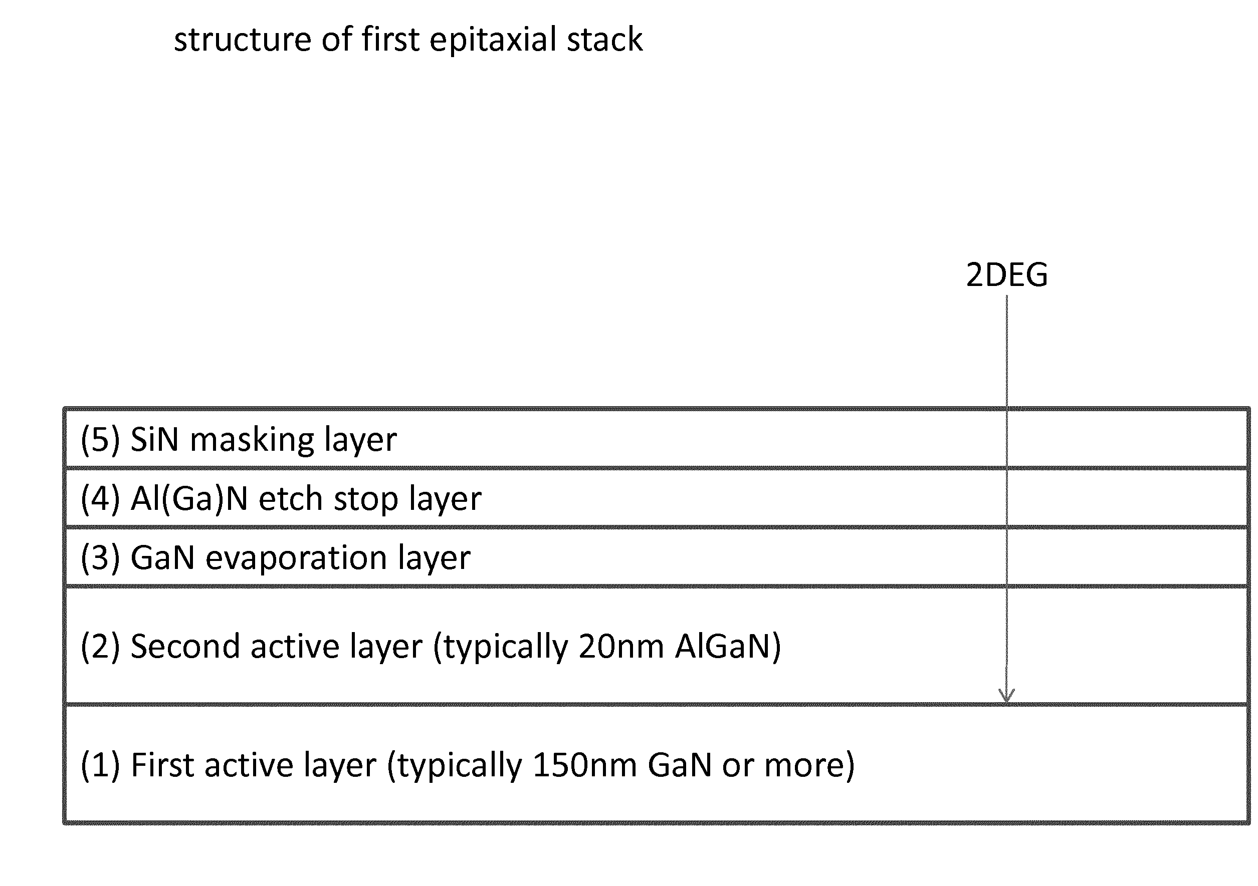
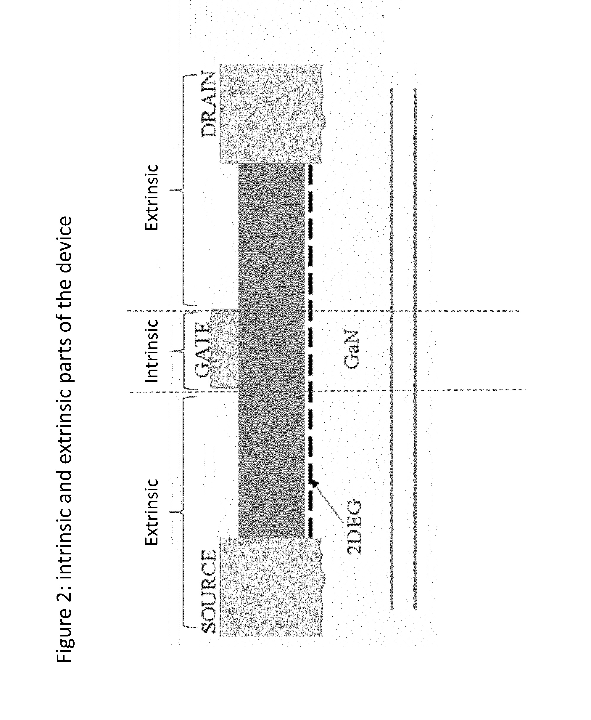
[0044]The present invention will be described with respect to particular embodiments and with reference to certain drawings but the invention is not limited thereto but only by the claims. The drawings described are only schematic and are non-limiting. In the drawings, the size of some of the elements may be exaggerated and not drawn on scale for illustrative purposes. The dimensions and the relative dimensions do not correspond to actual reductions to practice of the invention.[0045]It is to be noticed that the term “comprising”, used in the claims, should not be interpreted as being restricted to the means listed thereafter. Thus, the scope of the expression “a device comprising means A and B” should not be limited to devices consisting only of components A and B. It means that with respect to the present invention, the only relevant components of the device are A and B.[0046]Similarly, it is to be noticed that the term “coupled” should not be interpreted as being restricted to di...


PUM


Abstract

Disclosed are methods of growing III-V epitaxial layers on a substrate, a semiconductor structure comprising a substrate, a device comprising such a semiconductor structure, and an electronic circuit. Group III-nitride devices, such as, for example, high-electron-mobility transistors, may include a two-dimensional electron gas (2DEG) between two active layers. For example, the 2DEG may be between a GaN layer and a AlGaN layer. These transistors may work in depletion-mode operation, which means the channel has to be depleted to turn the transistor off. For certain applications, such as, for example, power switching or integrated logic, negative polarity gate supply is undesired. Transistors may then work in enhancement mode (E-mode).

Description

FIELD OF THE INVENTION[0001]The present invention relates to a method of growing III-V epitaxial layers on a substrate, a semiconductor structure comprising a substrate, a device comprising such a semiconductor structure, and an electronic circuit.TECHNICAL BACKGROUND[0002]Group III-V devices, such as e.g. HEMTs, comprise a 2DEG (two dimensional Electron Gas) between two active layers, e.g. between a GaN and a AlGaN layer. It is known that this 2DEG results from spontaneous and piezo-electric polarization leading to charge separation within the materials. In most known devices of this type, the 2DEG is present at zero gate bias due to the characteristics of the materials. GaN FET devices for instance, with contacts formed on top of an AlGaN barrier layer, are normally-on devices. It is assumed that the formation of contacts on top of the epitaxial structure does not change drastically the polarization charges in a heterostructure such that if a 2DEG were present before the formation...

Claims


Application Information

Patent Timeline
Patent Type & Authority Applications(United States)
IPC IPC(8): H01L29/778H01L29/66
CPCH01L29/66462H01L29/7786H01L29/2003H01L29/1066H01L29/66431H01L29/778
Inventor DERLUYN, JOFFDEGROOTE, STEFANGERMAIN, MARIANNE
Owner EPIGAN NV
Why Eureka
Try Eureka