

Back contacts for thin film solar cells
a solar cell and back contact technology, applied in the direction of climate sustainability, sustainable manufacturing/processing, semiconductor devices, etc., can solve the problems of affecting the annual production of cigs and cdte solar panels, low absorption coefficient of crystalline silicon, and high cost of crystalline silicon solar cell technologies, etc., to achieve good adhesion, high reflectivity, and high conductivity
- Summary
- Abstract
- Description
- Claims
- Application Information
AI Technical Summary
Benefits of technology
Problems solved by technology
Method used
Image

Examples
Embodiment Construction
[0024]A detailed description of one or more embodiments is provided below along with accompanying figures. The detailed description is provided in connection with such embodiments, but is not limited to any particular example. The scope is limited only by the claims and numerous alternatives, modifications, and equivalents are encompassed. Numerous specific details are set forth in the following description in order to provide a thorough understanding. These details are provided for the purpose of example and the described techniques may be practiced according to the claims without some or all of these specific details. For the purpose of clarity, technical material that is known in the technical fields related to the embodiments has not been described in detail to avoid unnecessarily obscuring the description.
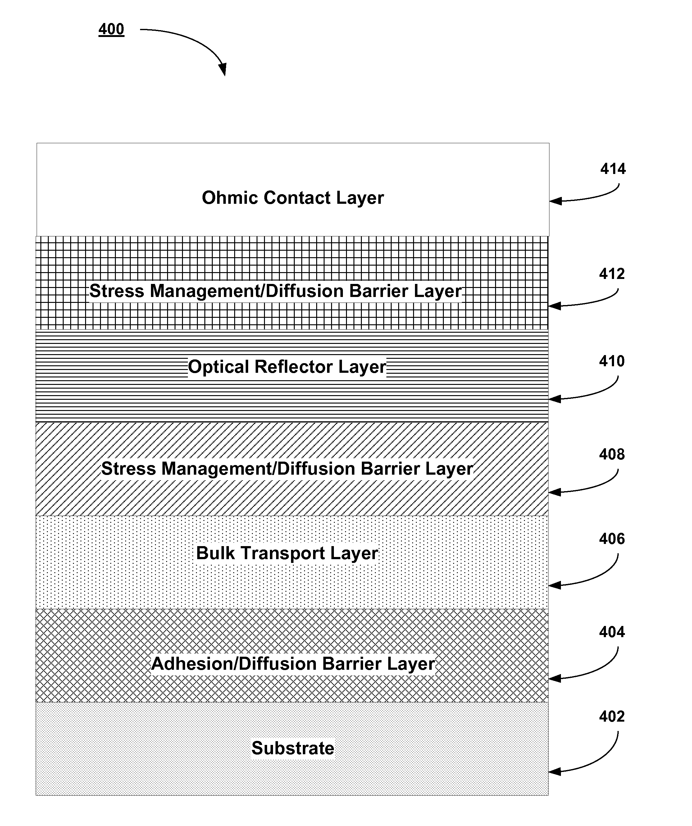
[0025]A general class of PV absorber films of special interest is formed as multinary compounds from Groups IB-IIIA-VIA of the periodic table. Group IB includes Cu, Ag, and Au...
PUM
 Abstract
Description
Claims
Application Information