Semiconductor light emitting device

a technology of semiconductors and light emitting devices, which is applied in the manufacture of semiconductor/solid-state devices, semiconductor devices, electrical devices, etc., can solve the problems of absorbing and losing the majority of light emitted and advanced toward the substrate, and the increase in the efficiency of deriving light is small in actuality, so as to achieve the effect of increasing the brightness of the semiconductor light emitting devi

Inactive Publication Date: 2006-03-28
ROHM CO LTD
View PDF4 Cites 37 Cited by
  • Summary
  • Abstract
  • Description
  • Claims
  • Application Information

AI Technical Summary

Benefits of technology

[0006]The present invention is directed in view of the above described situation, and an object of the present invention is to provide a structure of a light emitting device in which the brightness of the semiconductor light emitting device can be further increased, the light emitting device being formed by adhering a semiconductor layered portion having a light emitting layer forming portion made of compound semiconductor, to a conductive substrate via a metal layer.

Problems solved by technology

There is a problem that most of the light emitted and advanced toward the substrate is absorbed and lost in the above structure, because GaAs of the substrate is a material that absorbs light emitted in the light emitting layer forming portion 3.
As a result of research by the present inventors concerning the efficiency of deriving light in the above described structure shown in FIG. 4, however, it has been found that the increase in the efficiency of deriving light is slight in actuality, taking into consideration the time and effort needed to replace the substrate.

Method used


Image

  • Semiconductor light emitting device
  • Semiconductor light emitting device
  • Semiconductor light emitting device

Examples


Embodiment Construction

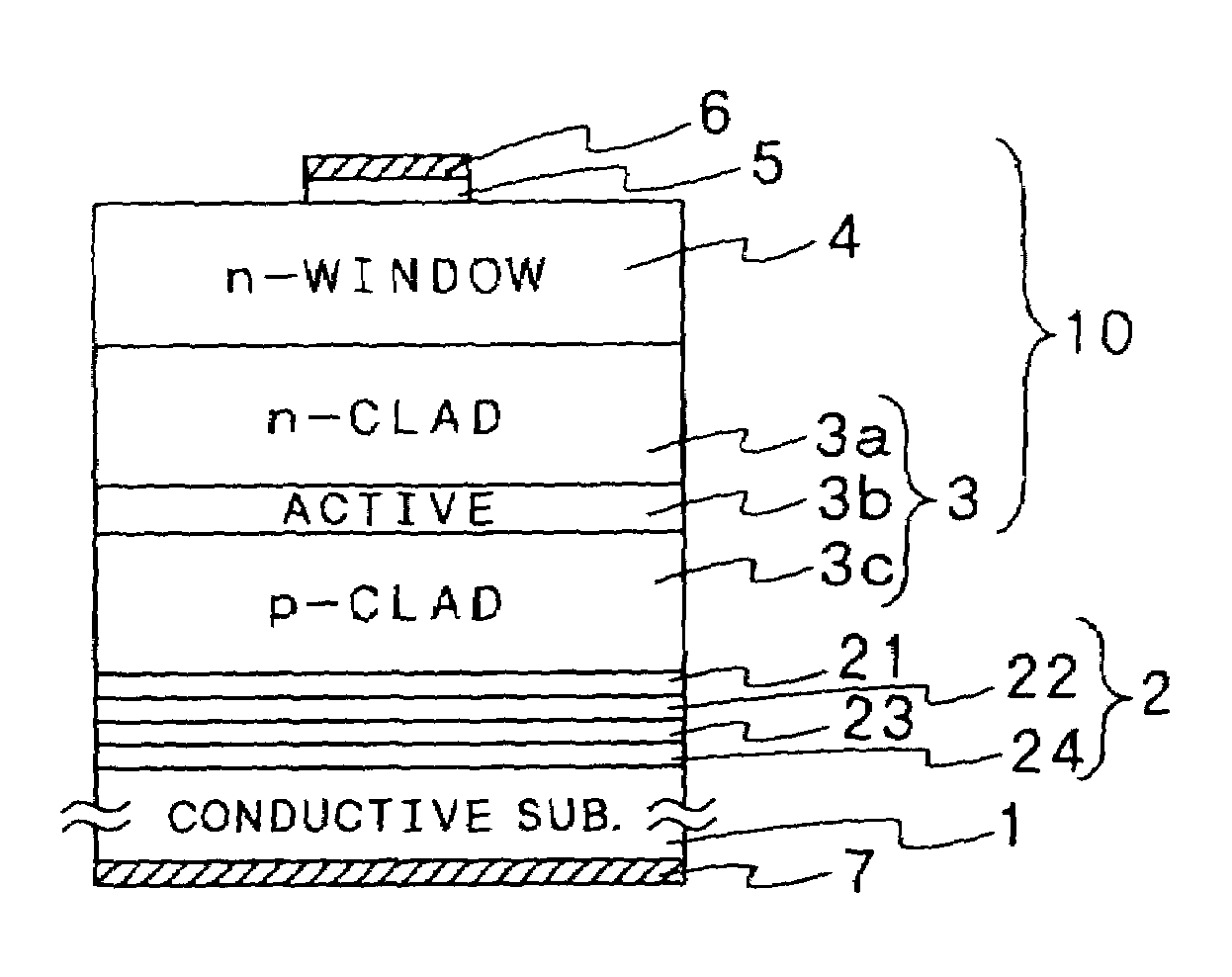
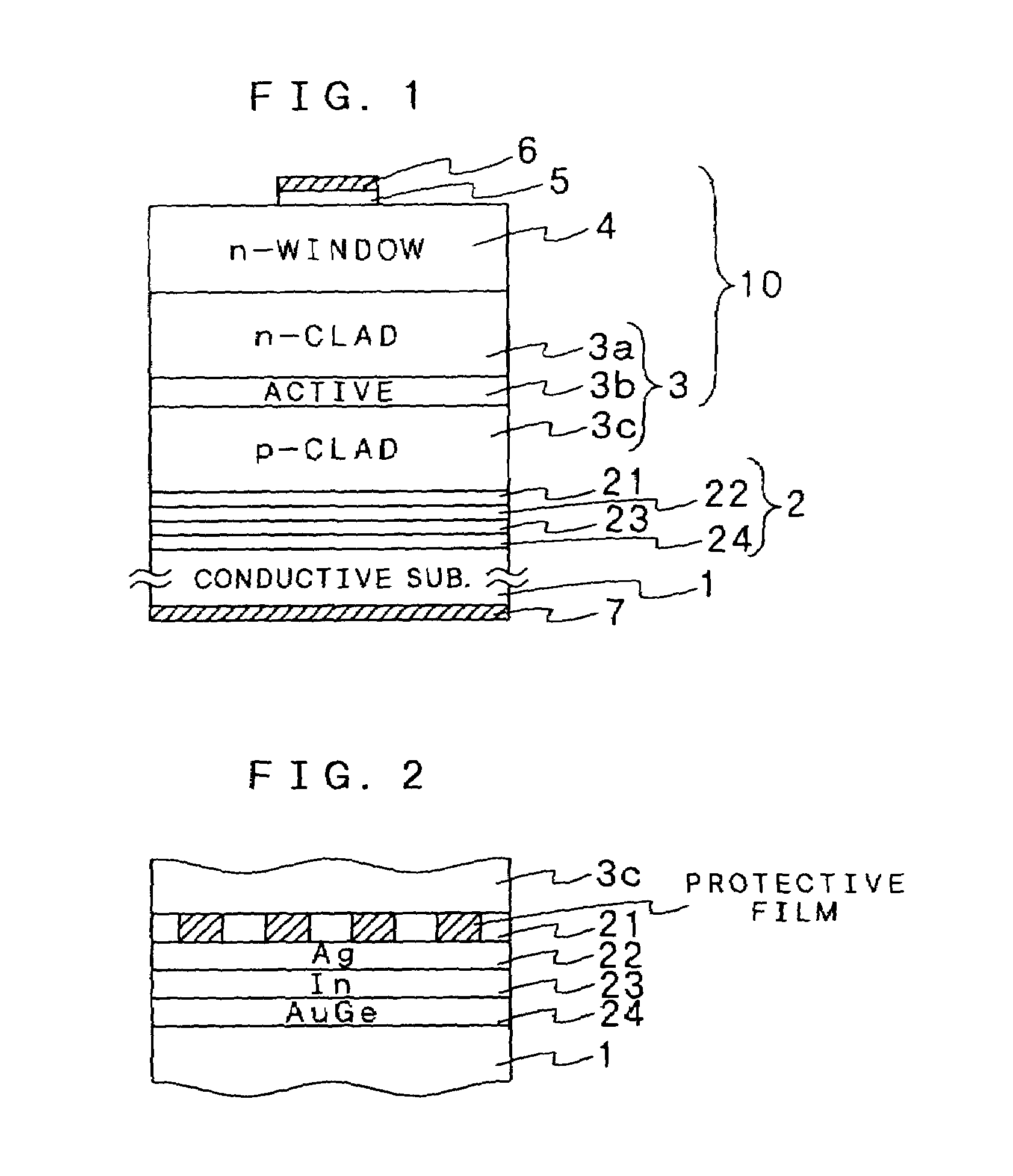
[0020]Next, a semiconductor light emitting device according to the present invention is described in reference to the drawings. A semiconductor light emitting device according to the present invention is formed by adhering a semiconductor layered portion 10 having a light emitting layer forming portion 3 to a conductive substrate 1 via a metal layer 2 as shown in the cross sectional structure of an LED chip in FIG. 1 which is one embodiment of the present invention. The present invention is characterized in that a metal layer 2 has at least a first metal layer 21 for making ohmic contact with the semiconductor layered portion 10, a second metal layer 22 made of Ag, and a third metal layer 23 made of a metal which allows adhesion to the conductive substrate 1 at a low temperature.

[0021]As described above, the present inventors have carried out diligent research in order to further enhance the brightness of the light emitting device, and as a result have discovered that semiconductor ...


PUM

PropertyMeasurementUnit
thicknessaaaaaaaaaa
thicknessaaaaaaaaaa
reflectanceaaaaaaaaaa

Abstract

A semiconductor light emitting device is formed by adhering a semiconductor layered portion having a light emitting layer forming portion to a conductive substrate via a metal layer. The metal layer has at least a first metal layer for ohmic contact with the semiconductor layered portion, a second metal layer made of Ag, and a third metal layer made of a metal which allows adhesion to the conductive substrate at a low temperature. As a result, the rate of reflection of light from the metal layer increases due to the presence of Ag in the metal layer. Further, the metal in the metal layer is prohibited from diffusing into the semiconductor layer, so that the semiconductor layer does not absorb light. And therefore the brightness of the semiconductor light emitting device can further be increased.

Description

FIELD OF THE INVENTION[0001]The present invention relates to a semiconductor light emitting device employed compound semiconductor material wherein a semiconductor layered portion, having a light emitting layer forming portion is adhered to a conductive substrate via a metal layer, and in particular to a semiconductor light emitting device wherein the efficiency of emitting light has been increased.BACKGROUND OF THE INVENTION[0002]In a conventional semiconductor light emitting device employing InGaAlP based compound semiconductor, for example, a semiconductor layered portion 10, in which a light emitting layer forming portion 3 having a double hetero-junction structure made of InGaAlP based semiconductor material, a window layer 4 made of AlGaAs based semiconductor material, and a contact layer 5 are laminated, is deposited on a semiconductor substrate made of GaAs. And a first electrode 6 made of an Au—Be alloy, or the like, is provided on the contact layer 5, and a second electrod...

Claims


Application Information

Patent Timeline
Patent Type & Authority Patents(United States)
IPC IPC(8): H01L29/06H01L21/28H01L33/30
CPCH01L33/405Y10S257/918
Inventor SHAKUDA, YUKIOMATSUMOTO, YUKIOOGURO, NOBUAKI
Owner ROHM CO LTD
Why Eureka
Try Eureka