

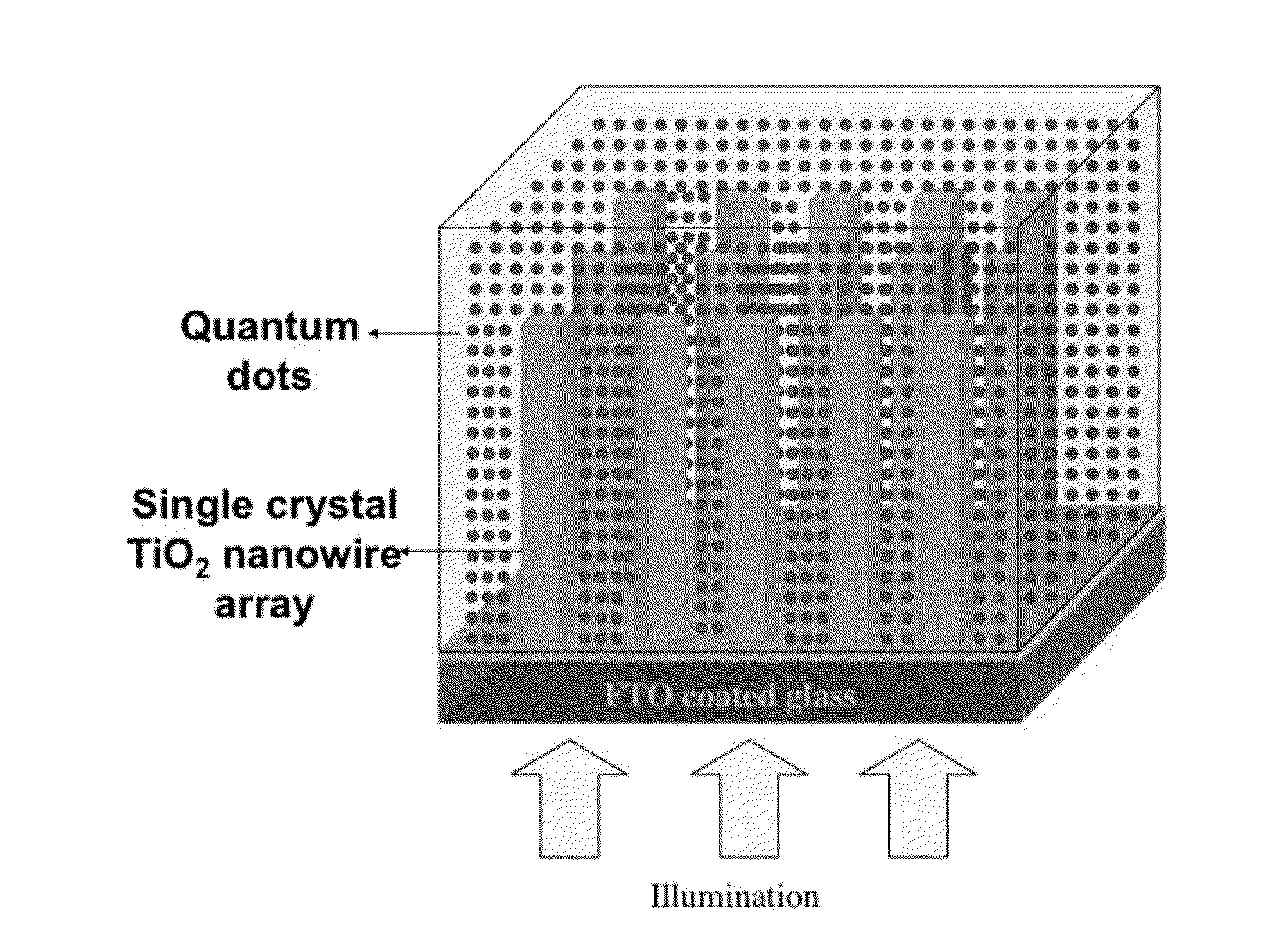
Methods to fabricate vertically oriented anatase nanowire arrays on transparent conductive substrates and applications thereof
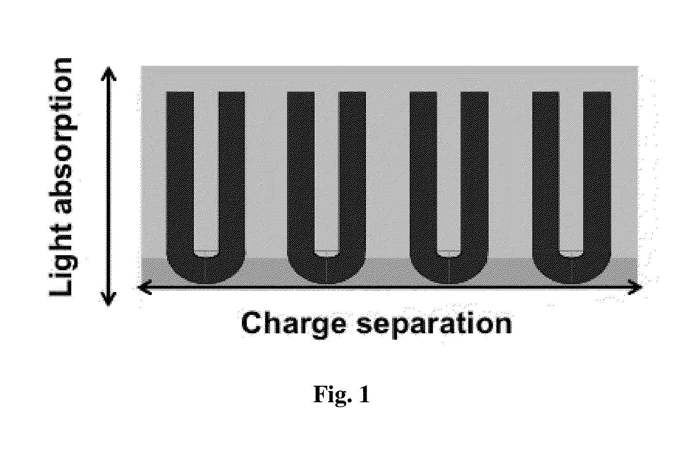
a technology of transparent conductive substrates and nanowire arrays, which is applied in the field of fabrication of crystalline anatase nanowire arrays vertically oriented from a substrate, can solve the problems of increasing series resistance, poor charge transport, and not achieving films, and achieves great utility and enhanced light absorption.
- Summary
- Abstract
- Description
- Claims
- Application Information
AI Technical Summary
Benefits of technology
Problems solved by technology
Method used
Image

Examples
example 1
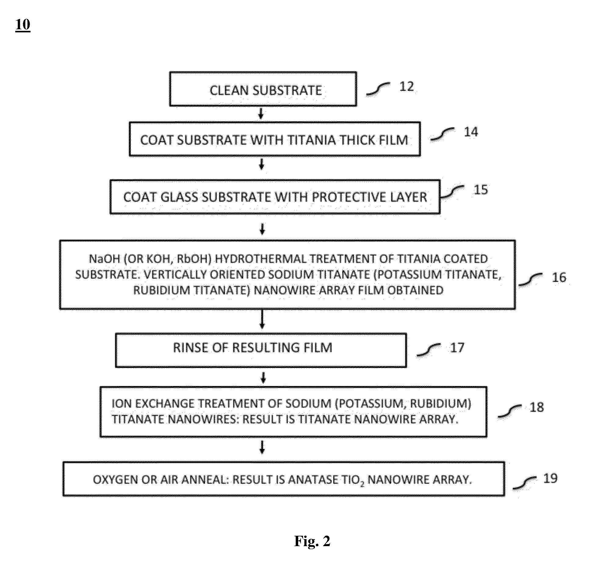
[0051]A dip-coating of the TCO-coated glass substrate in a TiO2 sol is used for deposition of the dense titania layer from which the anatase nanowire array will be fabricated. A TiO2 sol was made by dissolving 3 ml titanium tert-butoixde in 7 ml ethanol. For film deposition, the TCO-coated substrate was dipped into the sol, removed, then heated to evaporate the solvent, remove any organic materials on the surface, and promote densification of the deposited film (sintering of the multiple layers into one dense layer). In this example, the substrate was annealed after each sol-dipping step at 450° C. for 10 min Each dip-coating step resulted in an incremental film increase of approximately 100 nm, therefore for a desired starting thickness of 1 μm, ten dip-coating / annealing steps were used. Using a greater titanium butoxide sol concentration will give an incrementally thicker layer with each dip-coating. Using dip-coating, several micron thick titania films onto FTO-coated glass subst...
example 2
[0052]A TiO2 solution can be made using 0.1 g to 0.4 g of P25 nanoparticles in 10 ml of solvent which can be, for example, 3 ml titanium tert-butoixde in 7 ml ethanol. Solution dispersion is enhanced by stirring for an extended period, approximately 5-20 min. A FTO-glass substrate, immersed in the TiO2 solution, was used as the cathode and a platinum foil used as an anode. The distance between these two electrodes was 3 cm. 4 V DC bias was applied between these two electrodes for 3 min or longer depending on the density of the precursor solution and the film thickness needed. After deposition of the several micron thick TiO2 film, the substrate was taken out from the solution and annealed at 500° C. for 1 h to remove any residual organics. After this step, a protective Teflon coating was sprayed onto the back (non-TCO covered side) of the glass substrate.
Na2TiO4 Nanowire Array Fabrication by Hydrothermal Treatment of Titania Films
example 3
[0053]A FTO-glass substrate coated with a 12 μm thick dense titania layer was placed in a hydrothermal reactor containing 10 M NaOH for 2 h at 200° C. to convert the dense titania film into a 12 μm long Na2TiO4 nanowire array vertically oriented from the substrate. After removal from solution, the residual NaOH upon the surface of the film was removed by rinsing the sample in de-ionized water.
Na2TiO4 Nanowire Array Fabrication by Microwave Hydrothermal Treatment of Titania Films
PUM
| Property | Measurement | Unit |
|---|---|---|
| temperatures | aaaaa | aaaaa |
| power | aaaaa | aaaaa |
| power | aaaaa | aaaaa |
Abstract
Description
Claims
Application Information