Semiconductor device, its manufacture method and electronic component unit

a technology of semiconductor devices and electronic components, applied in semiconductor devices, semiconductor/solid-state device details, electrical apparatus, etc., can solve problems such as lowering reliability, and achieve the effects of improving quality, high quality, and improving tight adhesion

Inactive Publication Date: 2006-03-16
STANLEY ELECTRIC CO LTD
View PDF2 Cites 26 Cited by
  • Summary
  • Abstract
  • Description
  • Claims
  • Application Information

AI Technical Summary

Benefits of technology

[0023] This electronic component unit has a high quality and an improved tight adhesion during a heating process after bonding.
[0024] According

Problems solved by technology

The peeling becomes the rea

Method used


Image

  • Semiconductor device, its manufacture method and electronic component unit
  • Semiconductor device, its manufacture method and electronic component unit
  • Semiconductor device, its manufacture method and electronic component unit

Examples


Embodiment Construction

[0039] Studies on Japanese Patent Application No. 2003-088181 proposed by the present inventors have been made vigorously and the present application proposes a high quality semiconductor device, its manufacture method and an electronic component unit.

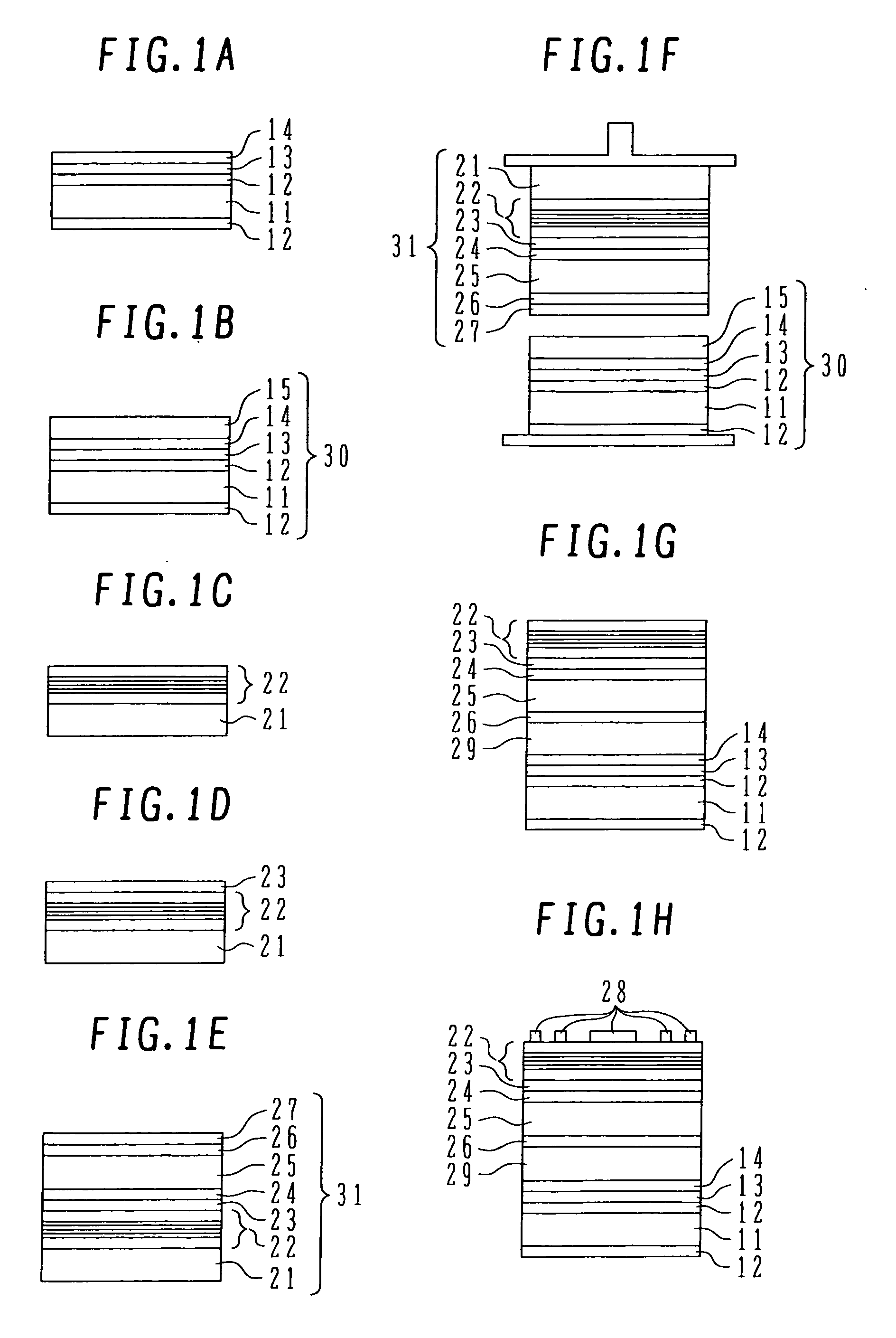
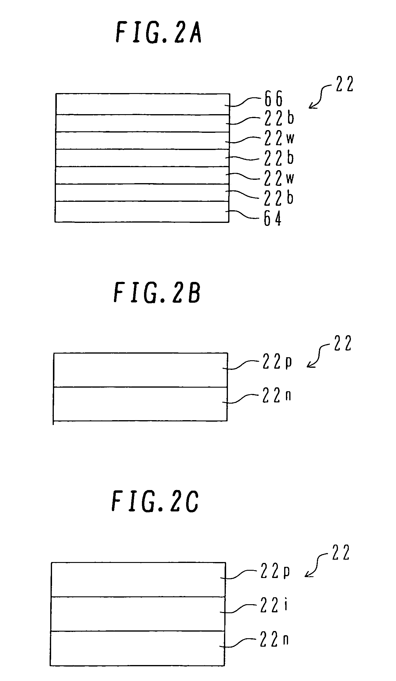
[0040]FIGS. 1A to 1H are schematic cross sectional views illustrating a manufacture method for a semiconductor light emitting device.

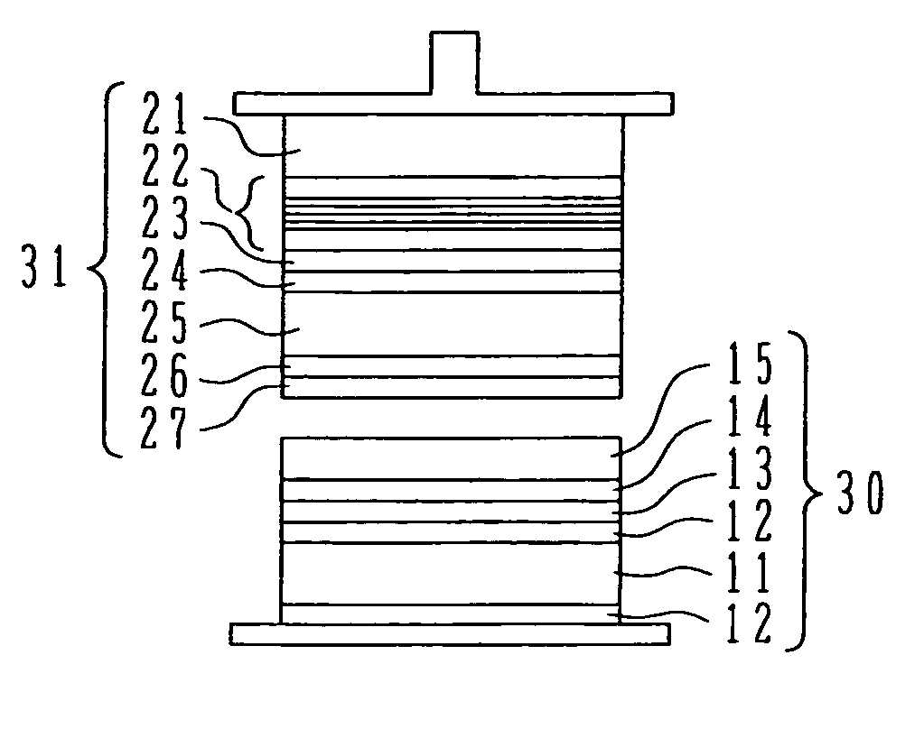
[0041] Reference is made to FIG. 1A. An Au layer 12 is formed on both surfaces of a conductive substrate 11, for example, made of Si with heavily doped n- or p-type impurities, by vapor deposition, and alloyed at 400° C. in a nitrogen atmosphere. A thickness of the Au layer 12 is, e.g., 150 to 600 nm. One of the Au layers 12 has a thickness of 150 nm and the other has a thickness of 600 nm. With this alloying process, the conductive substrate 11 are integrated with the Au layers 12, forming ohmic contacts.

[0042] It is therefore possible to prevent peeling of the Au layers 12 from the conductive substra...


PUM


Abstract

A LED chip having first and second electrodes on opposite principal surfaces, is bonded to a substrate through a composite bonding layer. The composite bonding layer is formed when a support substrate including the substrate and a first bonding layer is bonded to a lamination structure including the LED, the first electrode and a second bonding layer. The first or second bonding layer contains at least part of eutectic composition. At least one of the support substrate and the lamination structure includes a diffusion material layer. The composite bonding layer is formed in such a manner that eutectic material contents are mixed with the other to form a first mixture, and that the first mixture is mixed with diffusion material to form a second mixture having a melting point higher than a melting point of the first mixture.

Description

CROSS REFERENCE TO RELATED APPLICATION [0001] This application is based on and claims priority of Japanese Patent Application No.2004-267159 filed on Sep. 14, 2004, the entire contents of which are incorporated herein by reference. BACKGROUND OF THE INVENTION [0002] A) Field of the Invention [0003] The present invention relates to a semiconductor device, its manufacture method and an electronic component unit. [0004] B) Description of the Related Art [0005] Semiconductor light emitting devices have been proposed which have the structure that a semiconductor light emitting layer is bonded to a conductive substrate (for example, refer to Japanese Patent Laid-open Publication No. 2001-189490, No. 2001-44491, No. 2002-217450, No. HEI-5-251739, and U.S. Pat. No. 5,917,202, which are incorporated herein by reference). [0006]FIG. 19 is a schematic cross sectional view showing an example of a conventional semiconductor light emitting device 61 having the structure that a semiconductor light...

Claims


Application Information

Patent Timeline
IPC IPC(8): H01L21/30H01L21/00H01L33/10H01L33/30H01L33/40H01L33/62
CPCH01L33/0079H01L33/38H01L2224/92247H01L2224/73265H01L2224/48465H01L2224/48247H01L2224/32245H01L24/83H01L2924/01322H01L33/62H01L33/405H01L2924/00H01L2924/12036H01L2924/181H01L2224/48091H01L23/4827H01L24/29H01L2224/29124H01L2224/29144H01L2224/83075H01L2224/83203H01L33/0093H01L2924/00012H01L2924/00014H01L2924/0105
Inventor SONODA, JUNICHIKOBAYASHI, SEIICHIROYOSHIMIZU, KAZUYUKI
Owner STANLEY ELECTRIC CO LTD
Why Eureka
Try Eureka