Lateral device and preparation method for reducing influence of high-voltage interconnection

A lateral device, high-voltage technology, applied in semiconductor/solid-state device manufacturing, semiconductor devices, electrical components, etc., can solve the problems of device breakdown and the difficulty of complete depletion of the drift region, so as to improve the breakdown voltage and enhance the depletion capability. Effect

Active Publication Date: 2021-09-24
UNIV OF ELECTRONICS SCI & TECH OF CHINA +1
View PDF4 Cites 0 Cited by
  • Summary
  • Abstract
  • Description
  • Claims
  • Application Information

AI Technical Summary

Problems solved by technology

[0004] The invention aims at that in the high-voltage interconnection circuit, when the high-voltage interconnection line crosses the surface of the lateral device, the electric field lines are too concentrated in the local area of ​​the device, and induced charges are generated on the device surface, making it difficult to completely deplete the drift region, causing the device to occur in advance Breakdown issues, providing a lateral device that reduces the impact of high voltage interconnects

Method used


Image

  • Lateral device and preparation method for reducing influence of high-voltage interconnection
  • Lateral device and preparation method for reducing influence of high-voltage interconnection
  • Lateral device and preparation method for reducing influence of high-voltage interconnection

Examples


Embodiment 1

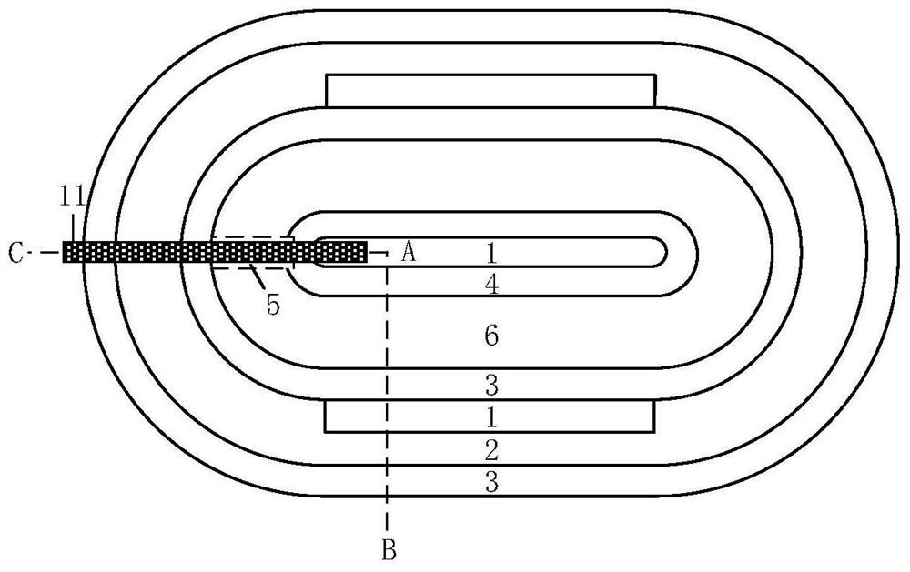
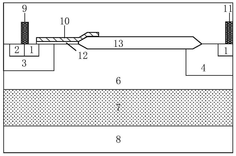
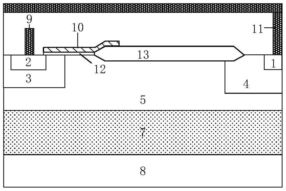
[0032] This embodiment provides a lateral device that reduces the influence of high-voltage interconnection, including a non-high-voltage interconnection structure and a high-voltage interconnection structure; the non-high-voltage interconnection structure is as follows figure 1 As shown in the cross-section of the AB line, the structure of the high-voltage interconnection area is as follows figure 1 The cross-section of the AC line in the center is shown;

[0033] The non-high-voltage interconnection region structure includes a second-type impurity-doped substrate 8, an insulating buried layer 7 formed on the second-type impurity-doped substrate 8, and a first-type impurity-doped epitaxial layer formed on the insulating buried layer 7. 6. On the left side of the first-type doped impurity epitaxial layer 6, a second-type doped impurity well region 3 is formed by ion implantation, and the first-type doped surface heavily doped inside the second-type doped impurity well region 3...

Embodiment 2

[0050] like Figure 4 As shown, the difference between this embodiment and Embodiment 1 is: when the first type doped impurity well region 4 is a first type doped impurity contact region 1, the lateral high voltage device is a lateral diffused metal oxide field When the effect transistor (LDMOS) is replaced by the second type doped impurity collector region 2, the lateral high voltage device is a lateral insulated gate bipolar transistor (LIGBT).

Embodiment 3

[0052] like Figure 5 As shown, the difference between this embodiment and Embodiment 1 is: the structure is an SOI structure, and this structure is a bulk silicon structure.


PUM

PropertyMeasurementUnit
thicknessaaaaaaaaaa

Abstract

The invention provides a lateral device and a preparation method for reducing the influence of high-voltage interconnection, comprising a first-type doped impurity contact region, a second-type doped impurity contact region, a second-type doped impurity well region, and a first-type doped impurity contact region. Impurity well region, first-type doped impurity drift region, first-type doped impurity epitaxial layer, insulating buried layer, second-type doped impurity substrate, source electrode, gate electrode, drain electrode, gate oxide layer, silicon part Oxidize the isolation oxide layer, respectively form the first-type doped impurity drift region of the high-voltage interconnection region and the first-type doped impurity epitaxial layer of the non-high-voltage interconnection region through different process steps, and change the drift region doping of the high-voltage interconnection region. The impurity concentration enhances the depletion capability of the drift region of the high-voltage interconnection region and improves the breakdown voltage of the device.

Description

technical field [0001] The invention belongs to the field of semiconductor power devices, and in particular relates to a lateral device that reduces the influence of high-voltage interconnection. Background technique [0002] With the great development of power semiconductor devices in the fields of power equipment and control circuits, the demand for power semiconductor devices will increase in the future. The advantage of power integrated circuits is the monolithic integration of high and low voltage devices, but it also brings severe challenges to circuit design. [0003] At present, most of the design styles of devices are runway type, which are mainly divided into two parts: high-voltage interconnection area and non-high-voltage interconnection area. regional structure. When a high-voltage interconnect line crosses the drift region of a high-voltage device such as a lateral double-diffused metal-oxide-semiconductor field-effect transistor LDMOS (Lateral Double-Diffuse...

Claims


Application Information

Patent Timeline
Patent Type & Authority Patents(China)
IPC IPC(8): H01L29/06H01L29/36H01L29/78H01L21/336H01L29/739H01L21/331
CPCH01L29/0615H01L29/36H01L29/66325H01L29/66681H01L29/7394H01L29/7823H01L29/7824
Inventor 周锌师锐鑫乔明张波
Owner UNIV OF ELECTRONICS SCI & TECH OF CHINA
Why Eureka
Try Eureka