
Method and device for transfer of data to or from a memory

A memory and data technology, applied in memory systems, static memory, digital memory information, etc., can solve the problems of unresolved electromagnetic interference effects, reduced transmission performance characteristics, and high production costs

Active Publication Date: 2018-03-13
STMICROELECTRONICS (GRENOBLE 2) SAS +1
View PDF5 Cites 3 Cited by
  • Summary
  • Abstract
  • Description
  • Claims
  • Application Information

AI Technical Summary

Problems solved by technology

[0010] Current solutions for attenuating EMI effects have the disadvantages of degrading transmission performance characteristics (such as, for example, 'slew rate' control), being effective only for clock signals (such as, for example, 'spread spectrum' techniques), or being expensive to produce (eg, for example, electromagnetic shielding)
[0011] In patent application US 2009 / 0086972 A1 a method for scrambling transmitted data has been provided, aiming at vertically scrambling the bits of each word according to a balanced distribution of "0"s and "1"s so that A solution to reduce power supply variations, but does not address the EMI effects created by the horizontal repetition of data patterns

Method used


Image

  • Method and device for transfer of data to or from a memory
  • Method and device for transfer of data to or from a memory
  • Method and device for transfer of data to or from a memory

Examples


Embodiment Construction

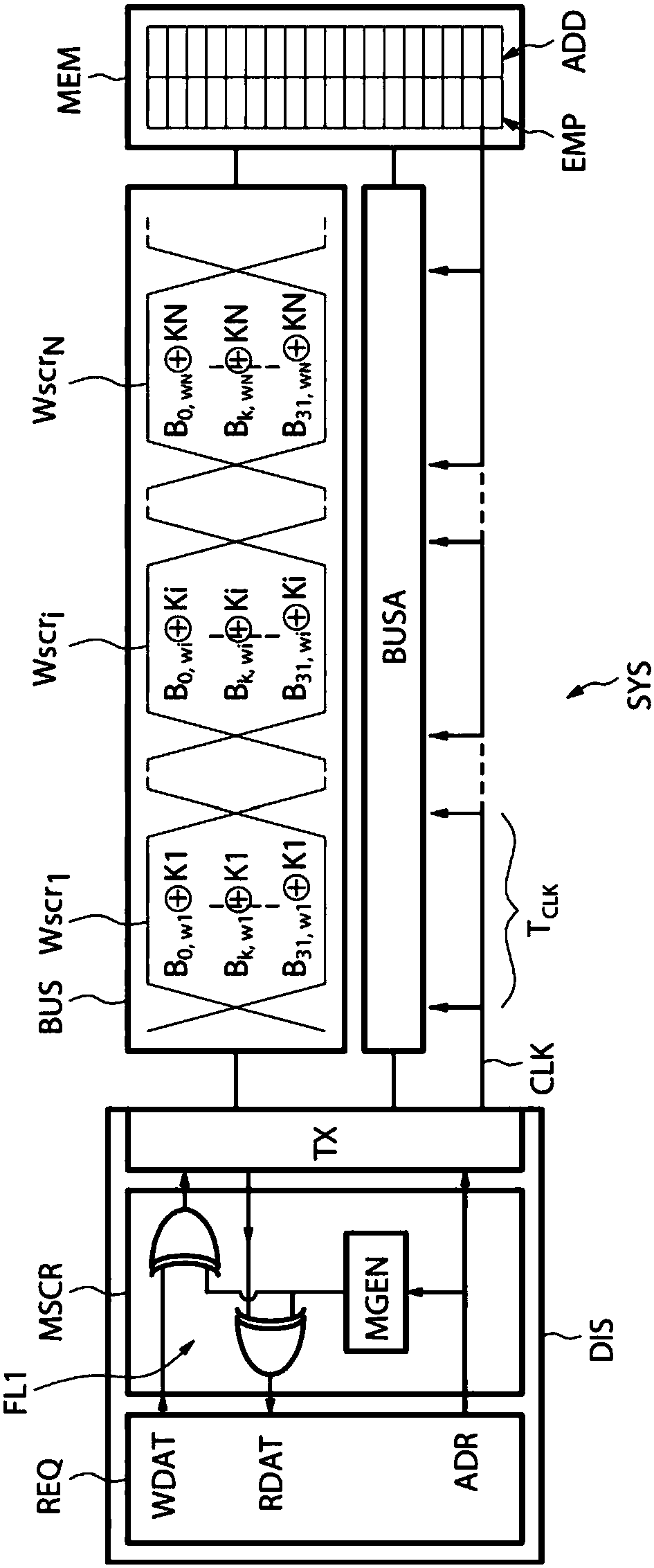
[0044] figure 1 An example of a system SYS is presented, comprising a system-on-chip arrangement DIS comprising, inter alia, a scrambling circuit MSCR and a transmission stage TX configured for communication with a dual data rate memory MEM for communication.

[0045] The scrambling circuit MSCR is configured for scrambling or descrambling data to be written or read at the memory location EMP with address ADD and comprises a signal generator MGEN and a first logic circuit CL1 .

[0046]For the sake of brevity, the term "address" will hereinafter denote both the memory location address and the memory location itself, as, for example, in the expression "write address".

[0047] The data to be transmitted is organized into words Wi (unscrambled words Wi are not shown in this figure), where 1≦i≦N, N depending on the protocol used, eg N=16. These words may, for example, each comprise 32 bits and are transferred successively each cycle TCLK of the clock signal CLK in order to be ...


PUM


Abstract

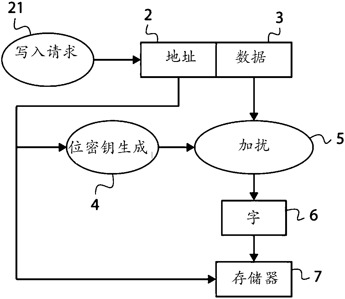
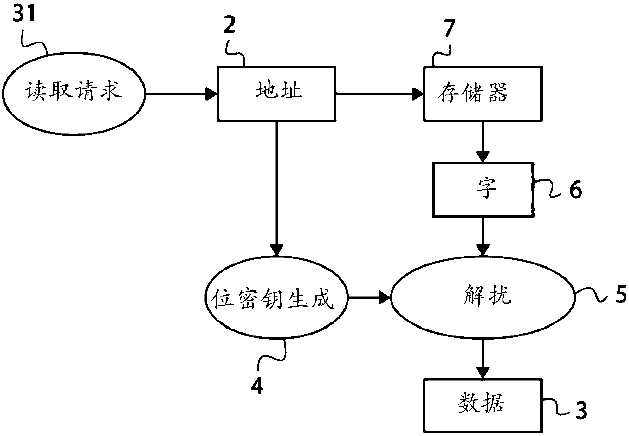
A method for reading or writing data at an address of a memory is disclosed. The data includes a number of consecutive words that each has a plurality of bits. The words are transferred to or from thememory in synchronization with a clock signal so that each word is transferred in one cycle of the clock signal. The bits are scrambled or unscrambled by applying a logic function to the bits of eachword. The logic function is identical for the scrambling and the unscrambling and makes use of a bit-key that is dedicated to the word and is identical for the scrambling and the unscrambling. Each bit-key comes from a pseudo-random series generated based on the address.

Description

[0001] Cross References to Related Applications [0002] This application claims priority from French Patent Application No. 1658232, filed September 5, 2016, which is hereby incorporated by reference. technical field [0003] Various embodiments of the present invention and implementations thereof relate to integrated circuits, and in particular to methods and apparatus for attenuating the effects of electromagnetic interference during transfer of data from or to a memory system, such as a double data rate memory. Background technique [0004] Access to double data rate (or DDR) memory, such as synchronous dynamic RAM memory (SDRAM) with double data rate, is typically accomplished through parallel high data rate links. [0005] Writing and reading data in DDR memory is typically performed by transferring a set of several words to or from consecutive memory locations, each word being transferred within one cycle of a clock signal. [0006] Each word consists of a number of...

Claims


Application Information

Patent Timeline
Patent Type & Authority Applications(China)
IPC IPC(8): G11C7/24
CPCG11C7/24G11C7/02G11C7/1006H04L9/0656H04L9/12G06F21/60G06F12/1408
Inventor A·古拉森P·德鲁埃
Owner STMICROELECTRONICS (GRENOBLE 2) SAS
Learn More