Shift register, driving method thereof, driving control circuit and related device

A technique for driving a control circuit and a shift register, which is applied in the fields of a drive control circuit, its driving method, a shift register, a display panel and a display device, and can solve problems such as the inability of a shift register to normally shift and output

Active Publication Date: 2018-03-30
SHANGHAI TIANMA MICRO ELECTRONICS CO LTD
View PDF8 Cites 32 Cited by
  • Summary
  • Abstract
  • Description
  • Claims
  • Application Information

AI Technical Summary

Problems solved by technology

[0004] An embodiment of the present invention provides a shift register, its driving method, a driving control circuit, a display panel, and a di

Method used


Image

  • Shift register, driving method thereof, driving control circuit and related device
  • Shift register, driving method thereof, driving control circuit and related device
  • Shift register, driving method thereof, driving control circuit and related device

Examples


Embodiment 1

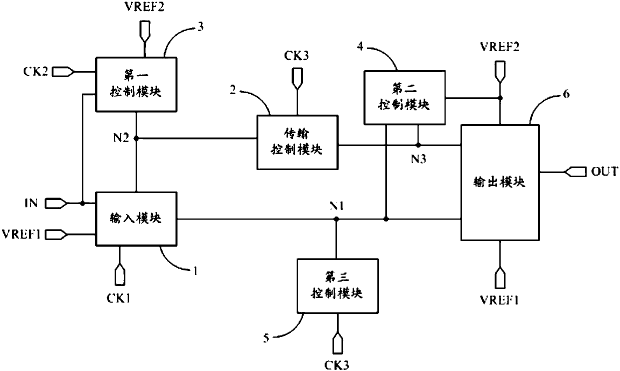
[0056] During specific implementation, in the shift register provided by the embodiment of the present invention, such as Figure 4 As shown, the input module 1 may include: a tenth transistor M10 and an eleventh transistor M11;

[0057] The control pole of the tenth transistor M10 is connected to the first clock signal terminal CK1, the first pole of the tenth transistor M10 is connected to the first reference signal terminal VREF1, and the second pole of the tenth transistor M10 is connected to the second node N2;

[0058] The control electrode of the eleventh transistor M11 is connected to the first clock signal terminal CK1 , the first electrode of the eleventh transistor M11 is connected to the input signal terminal IN, and the second electrode of the eleventh transistor M11 is connected to the first node N1 .

[0059] In the shift register provided by the embodiment of the present invention, when the tenth transistor is in a conducting state under the control of the sign...

Embodiment 2

[0093] by Figure 4 The structure of the shift register shown as an example, a T0 stage is inserted between the T4 stage and the T5 stage in the circuit timing diagram of the first embodiment, that is, on the basis of the circuit timing diagram in the first embodiment, the input signal terminal IN The duration of the high potential signal is extended by one clock cycle, and the corresponding circuit timing diagram is as follows Image 6 As shown, and mainly select eight stages of T1, T2, T3, T4, T0, T5, T6, and T7; among them, the T0 stage is divided into T01 sub-stage, T02 sub-stage and T03 sub-stage.

[0094] Because the structure of the shift register in the second embodiment is the same as that of the shift register in the first embodiment, and the potentials of the signals in the T1~T4 stages and T5~T7 stages in the circuit timing diagram in the second embodiment The corresponding potentials of the signals in the T1-T7 phases in the first embodiment are the same, therefo...

Embodiment 3

[0102] The structure of the shift register corresponding to this embodiment is as follows Figure 7 As shown, it is only for the first embodiment Figure 4 The connection mode of the first transistor M1 and the second transistor M2 in the transmission control module 2 is modified, so that the transmission control module can specifically be used to control the second node and the signal of the third clock signal terminal to control the first The signals of the three clock signal terminals are provided to the third node, so that the potential of the signal of the second node is the same as that of the signal of the third node. The connection modes of the remaining transistors are all the same as those in Embodiment 1. Figure 4 The same, and will not be repeated here.

[0103] During specific implementation, in the shift register provided by the embodiment of the present invention, such as Figure 7 As shown, in the transmission control module 2, the control pole of the first...


PUM


Abstract

The invention discloses a shift register, a driving method thereof, a driving control circuit, a display panel and a display device. Through arranging a third control module, stable signal of a firstnode is kept through controlling by the signal of the first node. In floating connection of the first node, the signal at a third clock signal end is coupled with the first node. When a signal outputend outputs an effective pulse signal, the signal of the first node is not affected by the signal at the third clock signal end, and influence of a second control module to the signal of a third nodeis prevented. Furthermore through arranging a transmission control module, the level of the signal of a second node is same with the level of the signal of the third node through controlling by the signal of a second node. The signal can be directly and quickly transmitted to the third node, thereby preventing a risk of signal transmission competition, and further preventing an output competitionrelation of the shift register so that the shift register can stably outputs the signal in a shifted manner.

Description

technical field [0001] The invention relates to the field of display technology, in particular to a shift register, its driving method, a driving control circuit, a display panel and a display device. Background technique [0002] An existing shift register, such as figure 1 As shown, it includes: transistors TFT1-TFT10, capacitors C01-C03. The corresponding timing diagram is as follows figure 2 As shown, in the shift phase t1, since the clock signal CK is at a low potential, both the transistor TFT1 and the transistor TFT2 are turned on. The turned-on transistor TFT2 makes the potential of the node N02 low, and the control transistor TFT6 turns on to charge the capacitor C02. Since the clock signal XCK is at a high potential, both the transistor TFT4 and the transistor TFT7 are turned off. The turned-on first transistor TFT1 makes the potential of the node N01 a low potential, so as to control both the transistor TFT8 and the transistor TFT10 to be turned on. The turn...

Claims


Application Information

Patent Timeline
IPC IPC(8): G09G3/20G09G3/3266G09G3/36G11C19/28
CPCG09G3/20G09G3/3266G09G3/3674G09G2310/0286G11C19/28
Inventor 冷传利李元
Owner SHANGHAI TIANMA MICRO ELECTRONICS CO LTD
Why Eureka
Try Eureka