Bootstrap sampling switch circuit, sample and hold circuit and time interleaved ADC
A technology of bootstrap sampling switch and time interleaving, which is applied in electrical components, analog/digital conversion, code conversion, etc., can solve the problems of large output clock jitter, complex structure, large timing deviation of clock signal, etc., to reduce jitter, structure Simple, Timing Mismatch Reduction Effects
- Summary
- Abstract
- Description
- Claims
- Application Information
AI Technical Summary
Problems solved by technology
Method used
Image

Examples
Embodiment 1
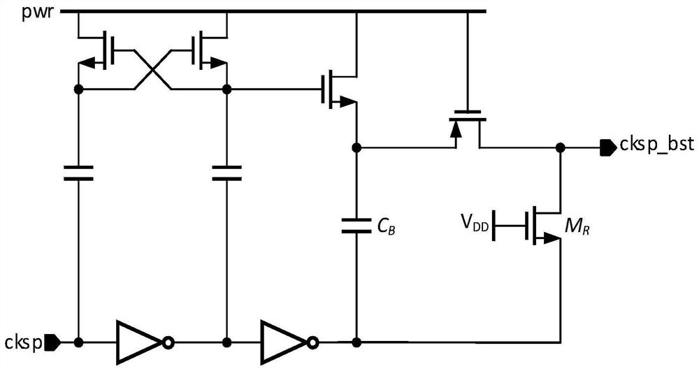
[0051] Such as Figure 4 As shown, this embodiment provides a bootstrap sampling switch circuit for time-interleaved ADC, the bootstrap sampling switch circuit includes a charge pump 3, a first capacitor C var , the first NMOS transistor N1, the first PMOS transistor P1, the first clock input terminal 4, the gate input terminal 5, the clock output terminal 6, the duty ratio adjustment circuit 1, the synchronization circuit 2, and the second NMOS transistor R var and the third NMOS tube M pd .
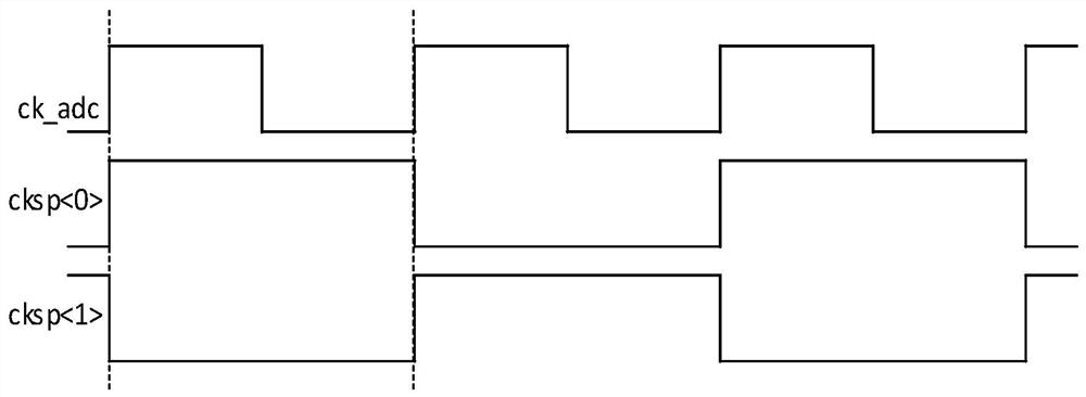
[0052] The strobe input terminal 5 is used to access the sampling selection signal sel of the i-th sub-ADC channel of the time-interleaved ADC , the first clock input terminal 4 is used to access the system clock ck_adc of the time-interleaved ADC, and the clock output terminal 6 is used to output the sampling clock signal cksp_bst , the sampling clock signal cksp_bst It is used to control the sampling switch of the sampling and holding circuit of the ith sub-ADC of the time-interle...
Embodiment 2
[0069] The difference between this embodiment and Implementation 1 is that the first capacitor C var use as Figure 9 The circuit shown is implemented. and Image 6 the difference is, Figure 9 The first capacitor C is controlled by controlling the reset level of the capacitor during the reset phase, that is, when the sel_int_n signal is high. var The equivalent capacitance value size. If the array capacitor C1 is selected, that is, the corresponding second control signal is high, the lower plate of the capacitor will be connected to the ground when it is reset, and the upper plate will be charged to the bias voltage pwr, so the array capacitor C1 The voltage is pwr. And if the array capacitor C1 is not selected, the lower plate is connected to pwr when reset, and the upper plate is also pwr, so the voltage of this capacitor is 0, similar to the fact that the array capacitor C1 does not exist.
Embodiment 3
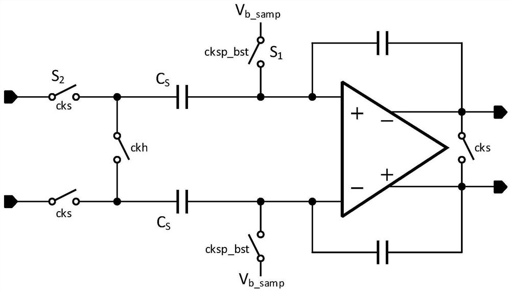
[0071] Such as Figure 10 As shown, this embodiment provides a sample-and-hold circuit for a sub-ADC in a time-interleaved ADC, and the sample-and-hold circuit includes a sampling switch S 3 And the bootstrap sampling switch circuit described in Embodiment 1, the sampling clock signal cksp_bst output by the clock output terminal used to control the sampling switch S 3 .
PUM
 Abstract
Description
Claims
Application Information