Automatic cell placement and optimization method for semi-custom back-end design of integrated circuits

A technology of integrated circuits and optimization methods, applied in CAD circuit design, computer-aided design, calculation, etc., can solve problems such as too long iteration time and poor design quality, so as to avoid invalid work, reduce the number of design iterations, and improve design quality effect

Active Publication Date: 2021-07-20
嘉兴倚韦电子科技有限公司
View PDF2 Cites 0 Cited by
  • Summary
  • Abstract
  • Description
  • Claims
  • Application Information

AI Technical Summary

Problems solved by technology

[0003] At present, there is no uniform and efficient automatic unit placement and optimization method in the industry, and the conventional design method has defects, mainly due to technical problems such as poor design quality and long iteration time, which are also needed in the current semi-customized back-end design. urgent technical problems

Method used


Image

  • Automatic cell placement and optimization method for semi-custom back-end design of integrated circuits
  • Automatic cell placement and optimization method for semi-custom back-end design of integrated circuits
  • Automatic cell placement and optimization method for semi-custom back-end design of integrated circuits

Examples


Embodiment Construction

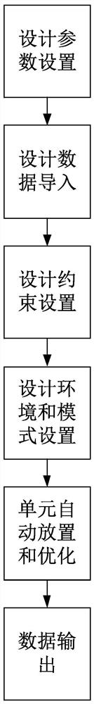
[0028] The invention discloses an automatic unit placement and optimization method for integrated circuit semi-customized back-end design. The specific implementation of the invention will be further described below in combination with preferred embodiments.

[0029] see attached figure 1 , figure 1 The specific flow of the automatic unit placement and optimization method for the integrated circuit semi-custom back-end design is shown. Preferably, the automatic unit placement and optimization method for semi-custom back-end design of integrated circuits includes the following steps:

[0030] Step S1: the back-end design tool defines the design parameters of the design environment model;

[0031] Step S2: The back-end design tool imports design constraint information according to unit placement requirements;

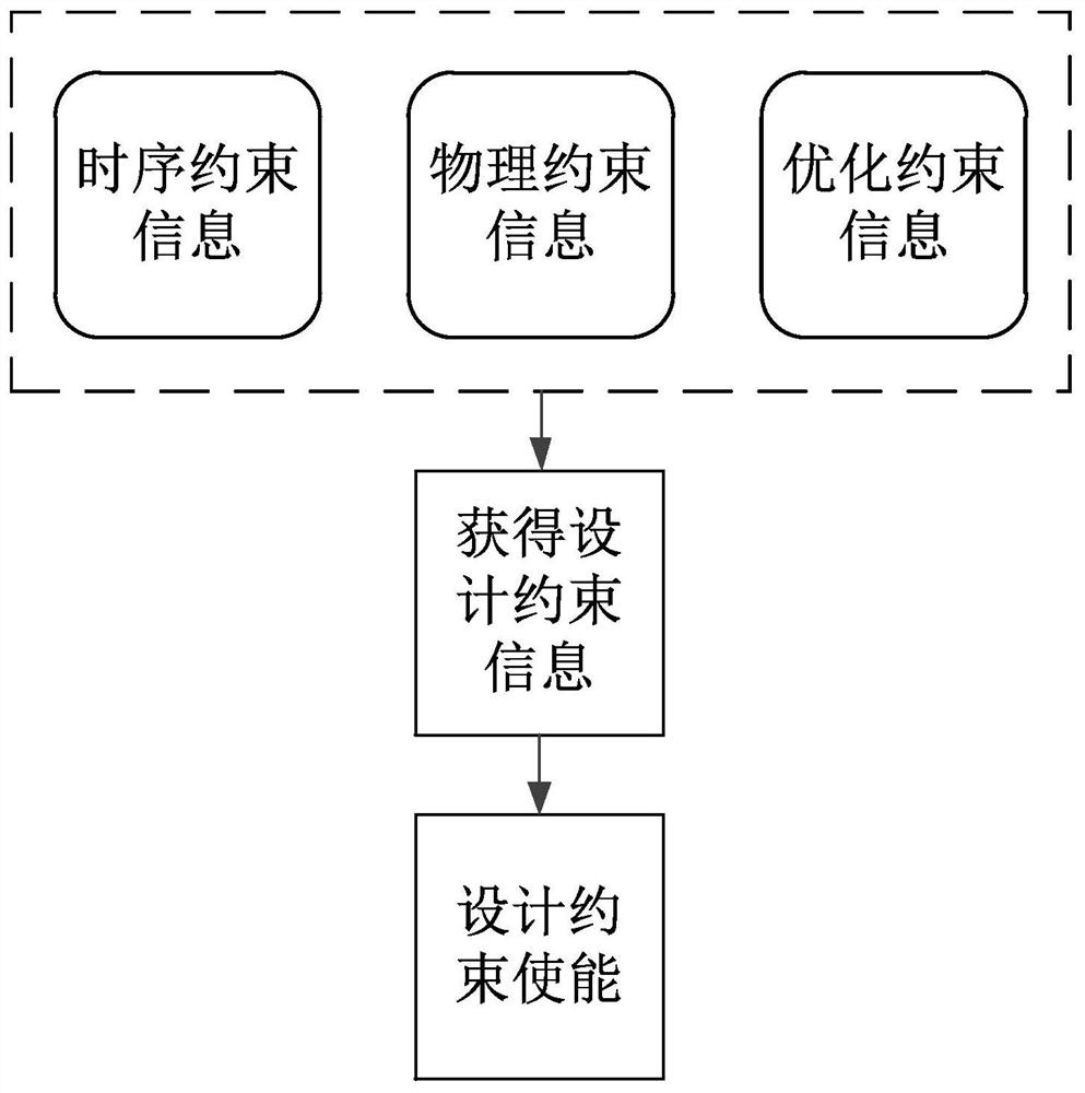
[0032] Step S3: The design constraint information module of the back-end design tool converts the above-mentioned design constraint information into the design constra...


PUM


Abstract

The invention discloses an automatic unit placement and optimization method for integrated circuit semi-customized back-end design. Step S1: the back-end design tool defines the design parameters of the design environment mode. Step S2: The back-end design tool imports design constraint information according to unit placement requirements. Step S3: The design constraint information module of the back-end design tool converts the above-mentioned design constraint information into the design constraint information of the preset format, and the design constraint enabling module of the back-end design tool simultaneously imports the above-mentioned design constraint information of the preset format into the back-end Fast cell placement module for design tools. The automatic unit placement and optimization method for integrated circuit semi-customized back-end design disclosed by the invention helps to improve the design quality of automatic unit placement, effectively avoids invalid work, reduces the number of design iterations, and shortens the entire chip design cycle.

Description

technical field [0001] The invention belongs to the technical field of design automation EDA in the integrated circuit design industry, and in particular relates to an automatic unit placement and optimization method for semi-customized back-end design of integrated circuits. Background technique [0002] In the field of design automation EDA technology in the integrated circuit design industry, automatic unit placement and optimization play an important role in the entire process of chip design, and the results are directly related to the final performance of the integrated chip. [0003] At present, there is no uniform and efficient automatic unit placement and optimization method in the industry, and the conventional design method has defects, mainly due to technical problems such as poor design quality and long iteration time, which are also needed in the current semi-customized back-end design. Urgent technical problems to be solved. Contents of the invention [0004...

Claims


Application Information

Patent Timeline
Patent Type & Authority Patents(China)
IPC IPC(8): G06F30/398G06F111/04
CPCG06F30/39G06F30/398G06F2111/04
Inventor 徐靖
Owner 嘉兴倚韦电子科技有限公司
Why Eureka
Try Eureka