

Silicon wafer texturing and transferring device
A technology for transfer devices and silicon wafers, which is applied in the directions of transportation and packaging, final product manufacturing, sustainable manufacturing/processing, etc., can solve problems such as the impact on the quality of silicon wafers, and achieve the effect of ensuring quality and avoiding edge chips
- Summary
- Abstract
- Description
- Claims
- Application Information
AI Technical Summary
Problems solved by technology
Method used
Image

Examples
Embodiment Construction
[0016] The present invention will be further described below in conjunction with the accompanying drawings and embodiments.
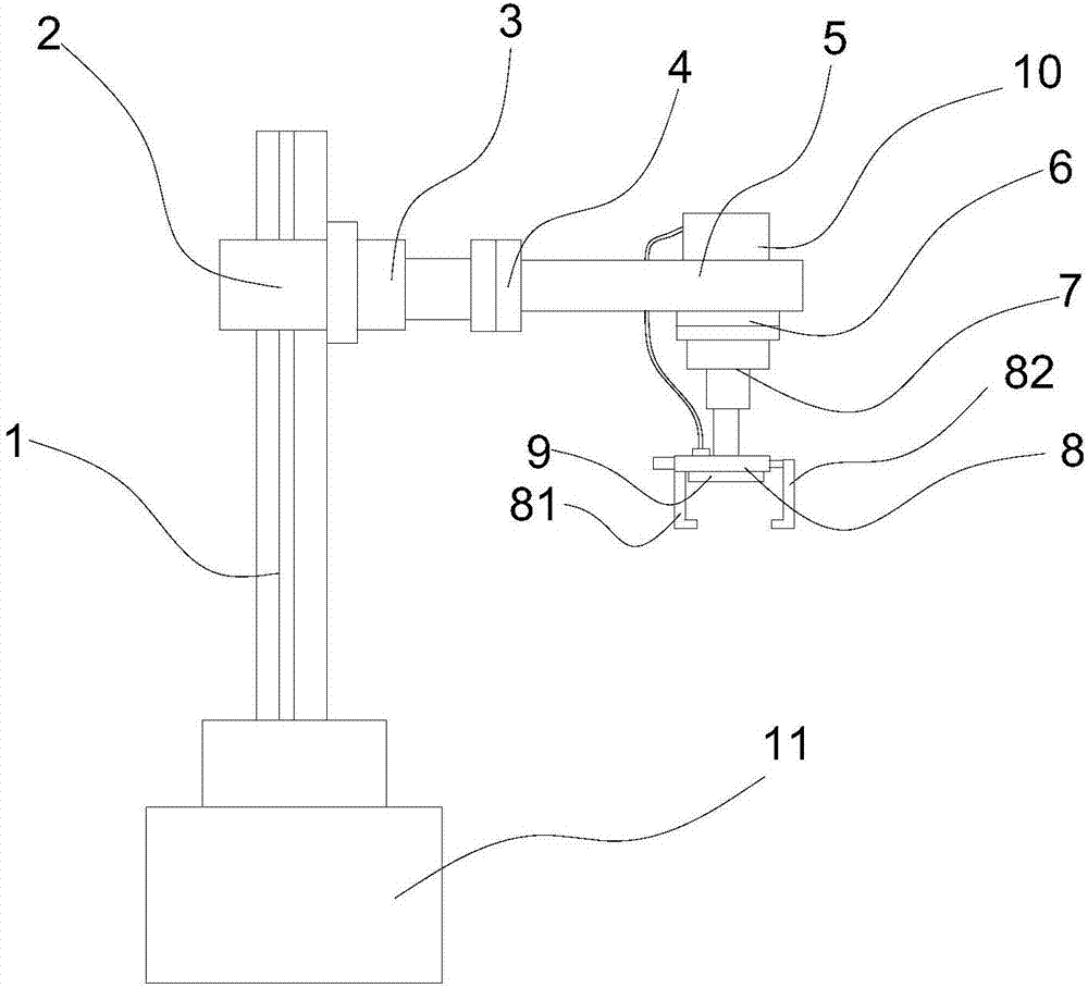
[0017] Such as Figure 1 to Figure 2 As shown, the silicon wafer texturing transfer device according to the present invention includes a mounting base 11, a turntable is arranged on the mounting base 11, a vertical sliding column 1 is installed on the rotating disk, and a vertical sliding column 1 is installed on the vertical sliding column 1. A slide table 2 is provided, and a first telescopic device 3 is arranged on the slide table 2. One end of the first telescopic device 3 is fixedly connected with the slide table 2, and the other end is provided with a support arm 5, and one end of the support arm 5 is connected to the The telescoping device 3 is connected by a rotating joint 4; a second turntable 6 is arranged below the other end of the support arm 5, and a second telescoping device 7 is arranged on the second turntable 6, and the lower end of the...
PUM
 Abstract
Description
Claims
Application Information