
Array substrate and its repairing method and liquid crystal display device

An array substrate and auxiliary electrode technology, applied in the field of array substrate and its repair method and liquid crystal display device, can solve the problems of poor image quality, limited increase in transmittance, flickering storage capacitor, etc., and achieve low power consumption and reduced The refresh rate and display effect are not affected

Active Publication Date: 2021-09-21
KUSN INFOVISION OPTOELECTRONICS
View PDF5 Cites 0 Cited by
  • Summary
  • Abstract
  • Description
  • Claims
  • Application Information

AI Technical Summary

Problems solved by technology

[0003] However, the above methods have the following problems: the improvement of transmittance is limited by resolution, color resistance materials, etc.; the current operating voltage of liquid crystal is already low, and it is difficult to lower it; the design of traditional AC common voltage drive (AV Vcom) Unable to perform column inversion and dot inversion, poor quality
[0004] According to p=1 / 2fcv 2 , P is the power, f is the refresh frequency, c is the capacitance, and v is the voltage. It can be seen that the power consumption of the liquid crystal display device is proportional to the refresh frequency, so the refresh frequency can be reduced to save power consumption when the picture is static, such as from 60HZ to 30HZ, but if the storage capacitor (Cs) of the liquid crystal display device is too small, there will be display problems such as flickering

Method used


Image

  • Array substrate and its repairing method and liquid crystal display device
  • Array substrate and its repairing method and liquid crystal display device
  • Array substrate and its repairing method and liquid crystal display device

Examples


no. 1 example

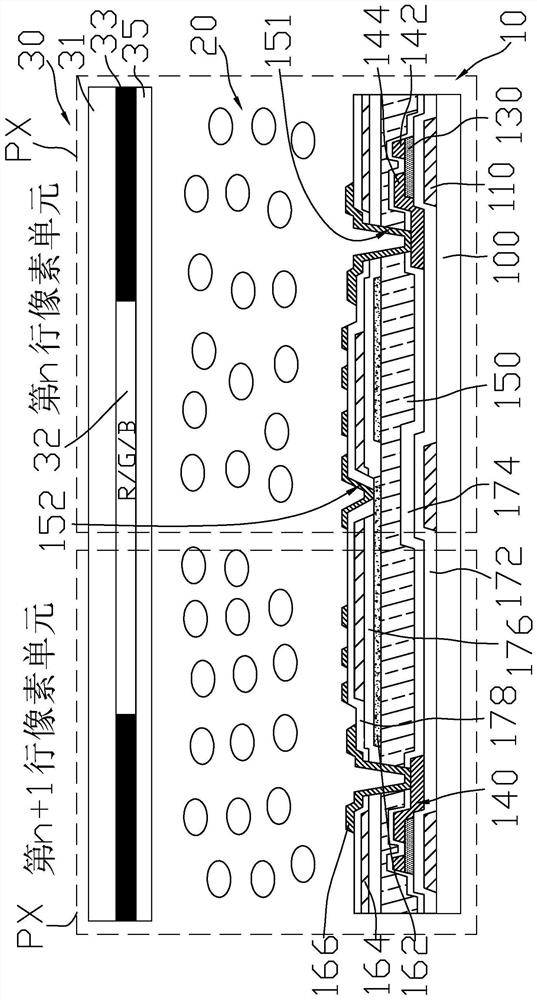
[0028] Such as figure 1 As shown, the liquid crystal display device of this embodiment includes an array substrate 10 , a liquid crystal layer 20 and a color filter substrate 30 , and the liquid crystal layer 20 is disposed between the array substrate 10 and the color filter substrate 30 .

[0029] Such as figure 1 and figure 2 As shown, the array substrate 10 includes a gate layer 110 , a source-drain layer 140 , a plurality of auxiliary electrodes 162 , a common electrode 164 and a plurality of pixel electrodes 166 . The gate layer 110 and the source-drain layer 140 are insulated from each other. The plurality of auxiliary electrodes 162, the common electrode 164 and the plurality of pixel electrodes 166 are spaced apart from each other, wherein the plurality of auxiliary electrodes 162 are located below the plurality of pixel electrodes 166, and the common electrode 164 is located under the plurality of pixel electrodes 166. Between the auxiliary electrode 162 and the p...

no. 2 example

[0039] Such as Figure 5 As shown, the liquid crystal display device of this embodiment includes an array substrate 10 , a liquid crystal layer 20 and a color filter substrate 30 , and the liquid crystal layer 20 is disposed between the array substrate 10 and the color filter substrate 30 .

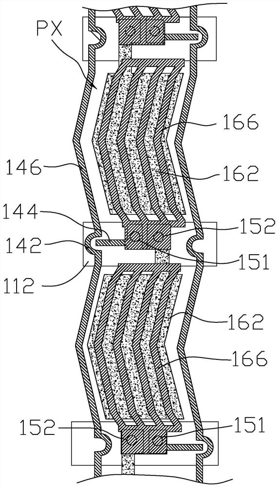
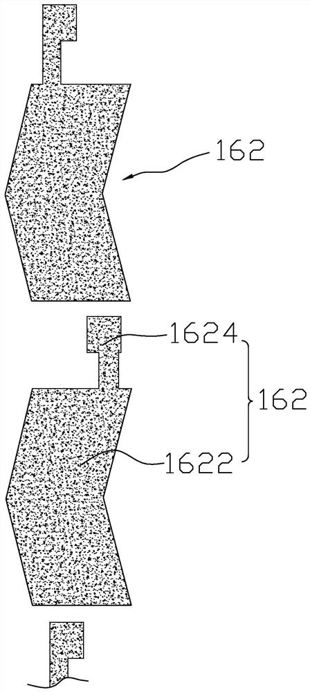
[0040] Such as Figure 5 and Figure 6 As shown, the structure of the array substrate 10 of this embodiment is the same as that of the above-mentioned first embodiment, the difference is that a method for repairing the array substrate 10 is also provided. In the array substrate 10 of this embodiment, the pixel electrode 166 in each pixel unit PX is conductively connected to the corresponding drain electrode 144 in the pixel unit PX through the first contact hole 151; in the upper and lower pixel units PX located in the same column, The pixel electrode 166 in the last pixel unit PX is conductively connected to the auxiliary electrode 162 in the next pixel unit PX through the second conta...

no. 3 example

[0043] Such as Figure 7 As shown, the liquid crystal display device of this embodiment includes an array substrate 10 , a liquid crystal layer 20 and a color filter substrate 30 , and the liquid crystal layer 20 is disposed between the array substrate 10 and the color filter substrate 30 .

[0044] Such as Figure 7 and Figure 8 As shown, the array substrate 10 includes a gate layer 110 , a source-drain layer 140 , a plurality of auxiliary electrodes 162 , a common electrode 164 and a plurality of pixel electrodes 166 . The gate layer 110 and the source-drain layer 140 are insulated from each other. The plurality of auxiliary electrodes 162, the common electrode 164 and the plurality of pixel electrodes 166 are spaced apart from each other, wherein the plurality of auxiliary electrodes 162 are located below the plurality of pixel electrodes 166, and the common electrode 164 is located under the plurality of pixel electrodes 166. Between the auxiliary electrode 162 and the...


PUM


Abstract

The invention discloses an array substrate, which includes a gate layer, a source drain layer, a common electrode, a plurality of pixel electrodes and a plurality of auxiliary electrodes, and among the plurality of auxiliary electrodes, the common electrode and the plurality of pixel electrodes The plurality of auxiliary electrodes are located at intervals between the plurality of pixel electrodes, the common electrode is located between the plurality of auxiliary electrodes and the plurality of pixel electrodes, and a plurality of pixels arranged in an array are formed on the array substrate. Each pixel unit is provided with an auxiliary electrode and a pixel electrode, and the source and drain layers include source and drain electrodes separated from each other. The pixel electrode in each pixel unit is connected to the pixel unit through the first contact hole. The corresponding drains are conductively connected; in the upper and lower pixel units located in the same column, the pixel electrode in the previous pixel unit is conductively connected with the auxiliary electrode in the next pixel unit through the second contact hole. The invention also discloses a method for repairing the array substrate and a liquid crystal display device.

Description

technical field [0001] The invention relates to the technical field of liquid crystal display, in particular to an array substrate, a repair method thereof, and a liquid crystal display device. Background technique [0002] With the rapid development of electronic products, consumers have higher and higher requirements for energy-saving products. For display panel manufacturers, the production of low-power consumption products has become a major challenge for them. In order to reduce the power consumption of liquid crystal display devices, the following solutions are usually adopted: 1. Increase the transmittance and reduce the power consumption of the backlight; 2. Use liquid crystal materials with high dielectric constants to reduce the panel driving voltage; 3. Use DC drive 4. Design a new pixel structure to reduce the liquid crystal operating voltage, thereby reducing panel power consumption. [0003] However, the above methods have the following problems: the improveme...

Claims


Application Information

Patent Timeline
Patent Type & Authority Patents(China)
IPC IPC(8): G02F1/13G02F1/1343G02F1/1362
CPCG02F1/1309G02F1/134309G02F1/136213G02F1/136227G02F1/136259G02F1/136286G02F1/134345
Inventor 钟德镇苏子芳李元莉
Owner KUSN INFOVISION OPTOELECTRONICS
Learn More