Electronic packaging material fake-prevention method and device

An electronic packaging material and packaging material technology, applied in the field of anti-counterfeiting, can solve the problems of inability to track and monitor, anti-counterfeiting technology is not real-time, etc.

Pending Publication Date: 2018-05-04
CHANGZHOU INST OF PRINTED ELECTRONICS IND CO LTD
View PDF0 Cites 0 Cited by
  • Summary
  • Abstract
  • Description
  • Claims
  • Application Information

AI Technical Summary

Problems solved by technology

However, these anti-counterfeiting technologies are not real-time and cannot be tracked and monitored

Method used


Image

  • Electronic packaging material fake-prevention method and device
  • Electronic packaging material fake-prevention method and device
  • Electronic packaging material fake-prevention method and device

Examples


no. 1 example

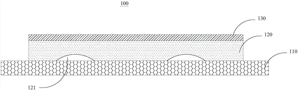
[0037] The embodiment of the present invention provides an anti-counterfeiting method for electronic packaging materials. The anti-counterfeiting method for electronic packaging materials is by adding a conductive layer 120 in the packaging material and adding a circuit easy-to-break point 121 in the conductive layer 120. When the packaging material is opened, the circuit The easy-to-break point 121 is disconnected to realize anti-counterfeiting.

[0038] see figure 1 The steps of adding a conductive layer 120 to the packaging material to realize anti-counterfeiting include:

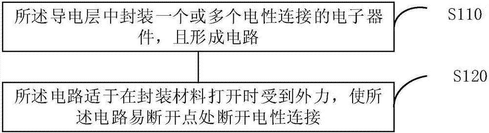
[0039] S110: Encapsulate one or more electrically connected electronic devices in the conductive layer, and form a circuit.

[0040] The conductive layer 120 encapsulates one or more electrically connected electronic devices. An electronic device, which can be, but is not limited to, an electrical wire, a resistor, a capacitor, an inductor, a diode, a transistor, a touch switch, a sensor electronic cir...

no. 2 example

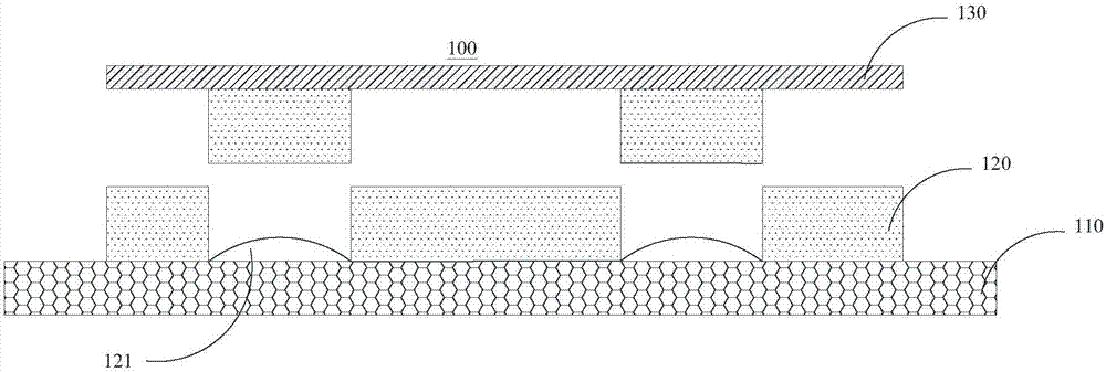
[0049] see figure 2 , the embodiment of the present invention provides an anti-counterfeiting device 100 . The anti-counterfeiting device 100 includes an encapsulation material with a conductive layer 120 inside; the conductive layer 120 includes at least one easily disconnected point 121;

[0050] The circuit easy-to-break point 121 is suitable for receiving an external force when the packaging material is opened, so as to change the circuit performance of the conductive layer 120 . The circuit break point 121 is suitable for changing the circuit performance of the conductive layer 120 when an external force is applied, so that the original packaging can be checked by electronic detection method.

[0051] Among them, the circuit easy-to-break point 121 can be, but not limited to, a single-layer circuit is disconnected, a multi-layer circuit is disconnected at the same point, a single-layer circuit is disconnected at different points, a multi-layer circuit is disconnected at...


PUM


Abstract

The invention relates to an electronic packaging material fake-prevention method and device. The electronic packaging material fake-prevention method comprises the steps of adding a conducting layer into a packaging material, adding circuit cut-off points into the conducting layer, and when the packaging material is opened, cutting off the circuit cut-off points to achieve fake prevention. By adding the conducting layer into the electronic packaging material and adding the circuit cut-off points into the conducting layer, after the electronic packaging material is damaged along the circuit cut-off points, the circuit state of the conducting layer is changed, and thus whether an original package is damaged or not can be detected through an electronic detecting method, and the purpose of fake prevention and dismantling prevention is achieved. Besides, when the electronic packaging material is installed and dismantled or squeezed and deformed violently, the damage degree can be judged byutilizing circuit performance (resistance) change caused by local separation or fracture of the conducting layer.

Description

technical field [0001] The invention relates to the field of anti-counterfeiting, in particular to an anti-counterfeiting method and device for electronic packaging materials. Background technique [0002] With the increase of imitation technology, how to identify the authenticity of products is an urgent need for consumers. In the prior art, commonly used packaging anti-counterfeiting technologies include barcodes, two-dimensional codes, optical anti-counterfeiting (laser holography), and special anti-counterfeiting materials (fluorescence, light-sensitive, heat-sensitive, moisture-sensitive, reactive color-changing, special materials). However, these anti-counterfeiting technologies are not real-time and cannot be tracked and monitored. [0003] How to solve the above problems is an urgent problem for manufacturers at present. Contents of the invention [0004] The object of the present invention is to provide an anti-counterfeiting method and device for electronic pac...

Claims


Application Information

Patent Timeline
Patent Type & Authority Applications(China)
IPC IPC(8): G06K19/077H01L23/31H01L23/58
CPCG06K19/07745H01L23/3107H01L23/58
Inventor 张婕宋李平张瑞国
Owner CHANGZHOU INST OF PRINTED ELECTRONICS IND CO LTD
Why Eureka
Try Eureka