Pixel definition layer, array substrate and display device
A pixel definition layer and array substrate technology, applied in the direction of electrical components, electrical solid devices, circuits, etc., can solve the problems of difficulty in meeting narrow frame design requirements, large frame occupation area, unfavorable narrow frame design requirements, etc., to achieve narrow frame Design, ensure the uniformity of film formation, and reduce the number of effects
- Summary
- Abstract
- Description
- Claims
- Application Information
AI Technical Summary
Problems solved by technology
Method used
Image

Examples
Embodiment 1
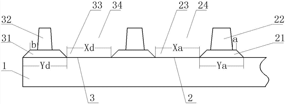
[0023] refer to figure 1 Shown is a schematic structural diagram of an embodiment of the pixel defining layer provided by the present invention. It can be seen from the figure that the pixel defining layer is usually disposed on the base substrate 1 for realizing the division and definition of the pixel units. Specifically, the pixel defining layer is composed of two layers of materials, including a first pixel defining layer (21, 31) and a second pixel defining layer (22) arranged on the first pixel defining layer (21, 31). , 32); Optionally, the first pixel defining layer (21, 31) is an inorganic pixel defining layer with lyophilic properties, for example, the material is selected from one of silicon dioxide, silicon nitride, silicon oxynitride or Various; the second pixel defining layer (22, 32) is an organic pixel defining layer with lyophobic properties, for example, the material is selected from fluorinated polyimide, fluorinated polymethyl methacrylate, polysiloxane, ...
Embodiment 2
[0029]When doing actual pixel design, refer to figure 1 As shown, the influencing factors that need to be considered in the design of the opening width Xa between the first pixel defining layers are resolution and the nature of the material; and the influencing factors that need to be considered in the designing of the width Ya of the first pixel defining layer are inkjet printing ink overflow popular. And Xa and Ya are usually designed to be equal in the prior art.
[0030] More specifically, take an 80ppi substrate as an example:
[0031] Suppose the pitch between pixel units is 314.16um, and the pitch between pixel subunits is 104.72um. In order to prevent the ink from overflowing into adjacent pixel subunits beyond the width Ya of the first pixel defining layer, Ya is greater than or equal to 15um;
[0032] The resolution of the opening width Xa between the first pixel-defining layers determines the spacing between pixels and pixel subunits, and the opening area of a ...
Embodiment 3
[0035] The width and height of the first pixel defining layer in the corresponding display area and the auxiliary area in the pixel defining layer are all the same, i.e. Yd=Ya. Similarly, the size of the corresponding opening area is also the same Xd=Xa; due to the application, the first pixel in the auxiliary area The width of the second pixel-defining layer 32 is smaller than the width of the second pixel-defining layer 22 in the display area, that is, the width b of the exposed first pixel-defining layer in the auxiliary area is greater than the width of the exposed first pixel-defining layer in the display area, resulting in b>a; in this way, during inkjet printing, the volume of ink printed in the corresponding pixels of the auxiliary area is greater than the volume of ink printed in the corresponding pixels of the display area.
[0036] In addition, based on the fact that the corresponding pixel defining layers in a display device are distributed in a quadrangular shape, ...
PUM
| Property | Measurement | Unit |
|---|---|---|
| Width | aaaaa | aaaaa |
Abstract
Description
Claims
Application Information