
Packaging module and formation method thereof

A technology for packaging modules and conductive substrates, which is used in the manufacture of electrical components, electrical solid-state devices, semiconductor/solid-state devices, etc. warping effect

Active Publication Date: 2018-05-15
HUAWEI DIGITAL POWER TECH CO LTD
View PDF7 Cites 1 Cited by
  • Summary
  • Abstract
  • Description
  • Claims
  • Application Information

AI Technical Summary

Problems solved by technology

However, in the current process of simultaneously embedding multiple chips into a packaging module, since there may be different height differences between the multiple chips, there are various blind holes of different depths in the packaging module. When the thickness of the chip mentioned above is relatively large (such as greater than 80 μm), there is a process capability limit and it is impossible to realize the filling operation of copper plating in the blind hole. Therefore, the current packaging module does not support the embedding of multiple chips of different thicknesses.

Method used


Image

  • Packaging module and formation method thereof
  • Packaging module and formation method thereof
  • Packaging module and formation method thereof

Examples


Embodiment Construction

[0053] The following will clearly and completely describe the technical solutions in the embodiments of the application with reference to the drawings in the embodiments of the application. Apparently, the described embodiments are only some of the embodiments of the application, not all of them. Based on the embodiments in this application, all other embodiments obtained by persons of ordinary skill in the art without making creative efforts belong to the scope of protection of this application.

[0054] In the following description, a lot of specific details are set forth in order to fully understand the application, but the application can also be implemented in other ways different from those described here, and those skilled in the art can do without violating the connotation of the application. By analogy, the present application is therefore not limited by the specific embodiments disclosed below.

[0055] As mentioned in the background technology section, in the curren...


PUM


Abstract

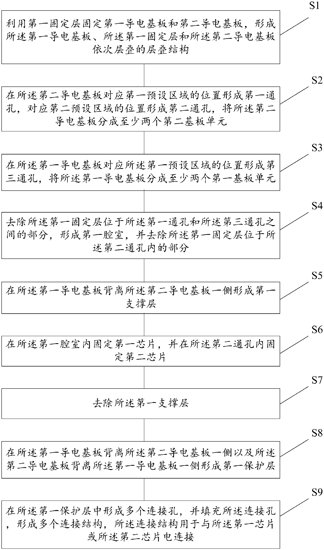
The embodiment of the invention discloses a packaging module and a formation method thereof. The method comprises the steps that a first conductive substrate and a second conductive substrate are fixed by using a first fixing layer so as to form a stacked structure; a first through hole is formed in the position corresponding to the first preset area of the second conductive substrate, and a second through hole is formed in the position corresponding to the second preset area; a third through hole is formed in the position corresponding to the first preset area of the first conductive substrate; the part between the first through hole and the third through hole of the first fixing layer is removed so that a first chamber is formed, and the part of the first fixing layer arranged in the second through hole is removed; and a first chip is fixed in the first chamber and a second chip is fixed in the second through hole so that different thickness of chips are installed through the first chamber and the second through hole which have different depth and the problem that the present packaging module does not support embedding of multiple different thickness of chips can be solved. The upper and lower parts of the packaging module are enabled to be balanced by the formation method so that the phenomenon of warping can be avoided.

Description

technical field [0001] The present application relates to the field of packaging technology, in particular to a packaging module and a forming method thereof. Background technique [0002] With the development of electronic products, the volume of packaging modules is getting smaller and higher, and the integration level is getting higher and higher. Therefore, the technology of embedding chips into substrates and realizing interconnection is developing more and more rapidly. However, in the current process of simultaneously embedding multiple chips into a packaging module, since there may be different height differences between the multiple chips, there are various blind holes of different depths in the packaging module. When the thickness of the above-mentioned chip is relatively large (for example, greater than 80 μm), there is a process capability limit and it is impossible to realize the filling operation of copper plating in the blind hole. Therefore, the current packa...

Claims


Application Information

Patent Timeline
Patent Type & Authority Applications(China)
IPC IPC(8): H01L21/56H01L21/60H01L23/31H01L23/535
CPCH01L21/56H01L23/31H01L23/535H01L24/01H01L2224/18
Inventor 廖小景侯召政王军鹤
Owner HUAWEI DIGITAL POWER TECH CO LTD
Learn More