LED filament substrate, LED package structure and LED lamp

A technology of LED filament and LED packaging, applied in lighting devices, lighting device components, lighting and heating equipment, etc., can solve the problems of limited chip type, chip spacing, series-parallel mode, single LED chip arrangement, etc. , to achieve the effect of diversifying the arrangement and more arrangement.

Active Publication Date: 2018-05-15
SHENZHEN REFOND OPTOELECTRONICS
View PDF4 Cites 45 Cited by
  • Summary
  • Abstract
  • Description
  • Claims
  • Application Information

AI Technical Summary

Problems solved by technology

[0003] In view of this, an embodiment of the present invention provides an LED filament substrate, an LED packaging structure, and an LED lamp to solve the limitations of the available chip types, chip spacing, and series-parallel connection of LED chips on the LED filament substrate in the prior art. The problem of single arrangement of LED chips

Method used


Image

  • LED filament substrate, LED package structure and LED lamp
  • LED filament substrate, LED package structure and LED lamp
  • LED filament substrate, LED package structure and LED lamp

Examples


Embodiment Construction

[0024] In the following description, specific details such as specific system structures and technologies are presented for the purpose of illustration rather than limitation, so as to thoroughly understand the embodiments of the present invention. It will be apparent, however, to one skilled in the art that the invention may be practiced in other embodiments without these specific details. In other instances, detailed descriptions of well-known systems, devices, circuits, and methods are omitted so as not to obscure the description of the present invention with unnecessary detail.

[0025] In order to illustrate the technical solutions of the present invention, specific examples are used below to illustrate.

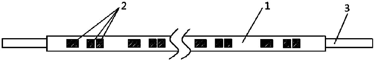
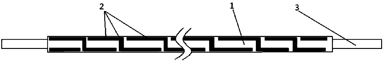
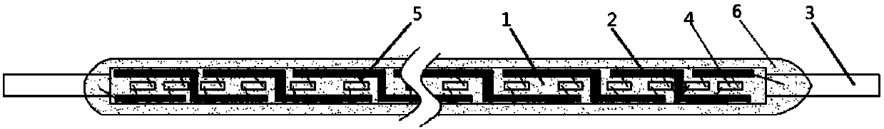
[0026] figure 1 It is a schematic structural diagram of an LED filament substrate provided by the first aspect of the embodiment of the present invention.

[0027] In the embodiment of the present invention, the LED filament substrate includes an insulating base mater...


PUM


Abstract

The invention is applicable to the technical field of light emitting diode applications, and provides an LED filament substrate, an LED package structure and an LED lamp. The LED filament substrate comprises an insulating substrate, conductive layers, and pins connected with an external power supply circuit. The conductive layers are arranged on the surface of the insulating substrate. The conductive layers are connected with external LED chips. The shape of the conductive layers is determined according to the type and connection mode of the external LED chips. The number of the conductive layers is determined according to the type and number of the external LED chips and the spacing between the external LED chips. The pins are arranged on the insulating substrate. According to the LED filament substrate, the LED package structure and the LED lamp, the conductive layers are arranged on the LED filament substrate; various types of LED chips can be selected; the spacing and series-parallel connection mode of the LED chips are not limited; and the arrangement of LED chips on the LED filament substrate is diversified.

Description

technical field [0001] The invention belongs to the technical field of light-emitting diode applications, and in particular relates to an LED filament substrate, an LED package structure and an LED lamp. Background technique [0002] At present, the typical structure of the insulating filament substrate is an insulating substrate and metal pins at both ends of the substrate for external electrical connection, and a plurality of light emitting diode (Light Emitting Diode, LED) chips arranged on the filament substrate can be selected Types, chip pitches, and series-parallel connections are all very limited. In the traditional packaging structure, usually a plurality of LED chips of the front-mounted structure are arranged in series on the substrate at equal intervals, and the arrangement of the chips is single. Contents of the invention [0003] In view of this, an embodiment of the present invention provides an LED filament substrate, an LED packaging structure, and an LED...

Claims


Application Information

Patent Timeline
Patent Type & Authority Applications(China)
IPC IPC(8): H01L33/62H01L33/48H01L25/075F21K9/90F21V19/00F21V23/00F21Y115/10
CPCF21K9/90F21V19/002F21V23/005F21Y2115/10H01L25/0753H01L33/48H01L33/62
Inventor 张丽君
Owner SHENZHEN REFOND OPTOELECTRONICS
Why Eureka
Try Eureka