Display substrate, manufacturing method thereof and display device
A technology for a display substrate and a manufacturing method, which is applied in the manufacturing of semiconductor/solid-state devices, electrical components, transistors, etc., can solve problems such as the influence of etching accuracy and the electrical characteristics of the semiconductor layer, and achieve the effect of easy etching accuracy.
- Summary
- Abstract
- Description
- Claims
- Application Information
AI Technical Summary
Problems solved by technology
Method used
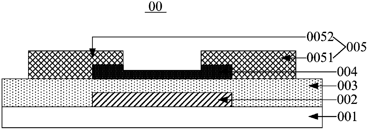
Image

Examples
Embodiment Construction
[0048] In order to make the purpose, technical solutions and advantages of the present invention clearer, the present invention will be further described in detail below in conjunction with the accompanying drawings. Obviously, the described embodiments are only some of the embodiments of the present invention, rather than all of them. Based on the embodiments of the present invention, all other embodiments obtained by persons of ordinary skill in the art without making creative efforts belong to the protection scope of the present invention.
[0049] With the progress of the manufacturing process of display products, new display technologies gradually replace the old thin film transistor liquid crystal display (English: Thin Film Transistor Liquid Crystal Display; abbreviation: TFT LCD) technology, for example, organic light-emitting diode (English: Organic Light-Emitting Diode (abbreviation: OLED) products are gradually replacing liquid crystal display products in the field o...
PUM
 Abstract
Description
Claims
Application Information