Array substrate, display device and preparation method of array substrate

An array substrate and dielectric layer technology, applied in semiconductor/solid-state device manufacturing, optics, instruments, etc., can solve problems such as abnormal electrical characteristics, SD metal wire breakage, dielectric layer breakage, etc., to improve ductility and flatness, prevent break effect

Inactive Publication Date: 2019-05-28
BOE TECH GRP CO LTD +1
View PDF6 Cites 6 Cited by
  • Summary
  • Abstract
  • Description
  • Claims
  • Application Information

AI Technical Summary

Problems solved by technology

[0003] 1. When laser stripping the Glass base, the laser energy is too high to irradiate P-Si (P-type silicon) and it is easy to cause abnormal electrical characteristics;
[0004] 2. When bending, it is easy to cause the dielectric layer to break and then cause the SD metal wire to break, and there will be a large number of point and line defects

Method used


Image

  • Array substrate, display device and preparation method of array substrate
  • Array substrate, display device and preparation method of array substrate
  • Array substrate, display device and preparation method of array substrate

Examples


Embodiment 1

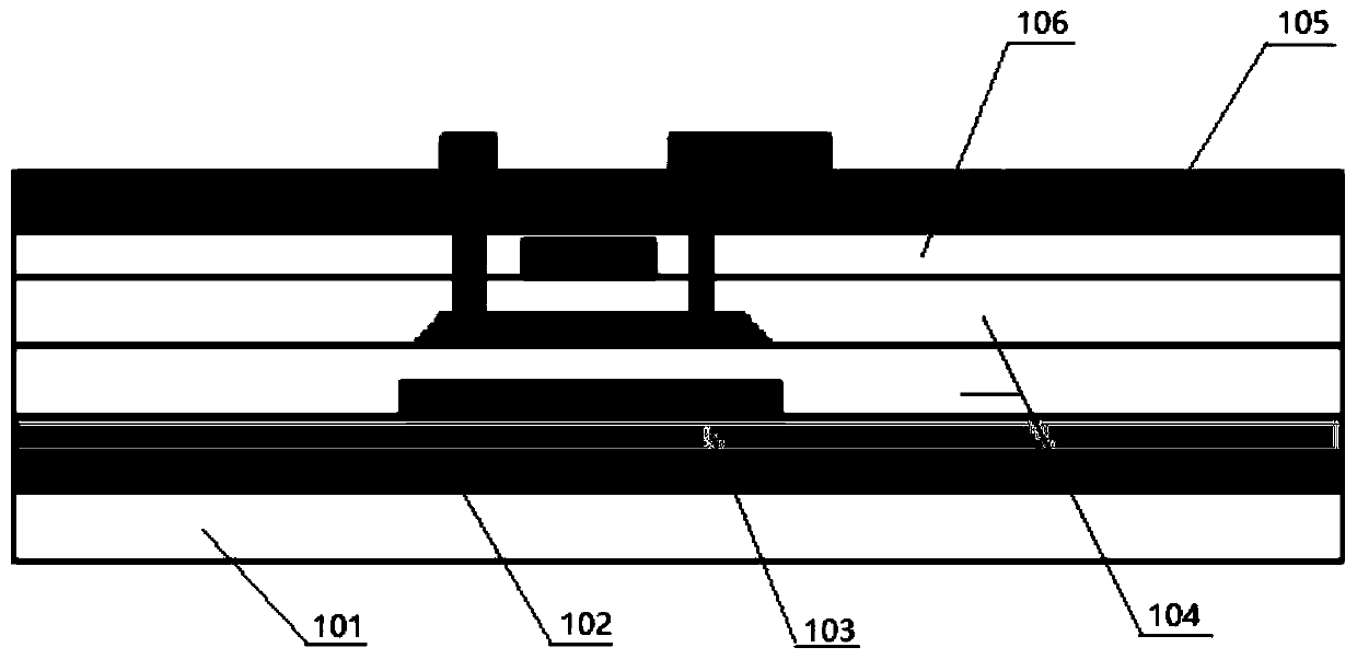
[0040] refer to figure 1 , shows one of the schematic diagrams of an array substrate of the present invention.

[0041] An embodiment of the present invention provides an array substrate, including a substrate 101, a PI layer 102, a protective layer 103, a thin film transistor layer 104, and a dielectric layer stacked on the substrate 101; wherein, the PI layer 102 is pasted attached to the substrate 101;

[0042] The dielectric layer includes an inorganic dielectric layer 106 and an organic dielectric layer 105 which are stacked.

[0043] In the embodiment of the present invention, the array substrate may be used in a flexible display.

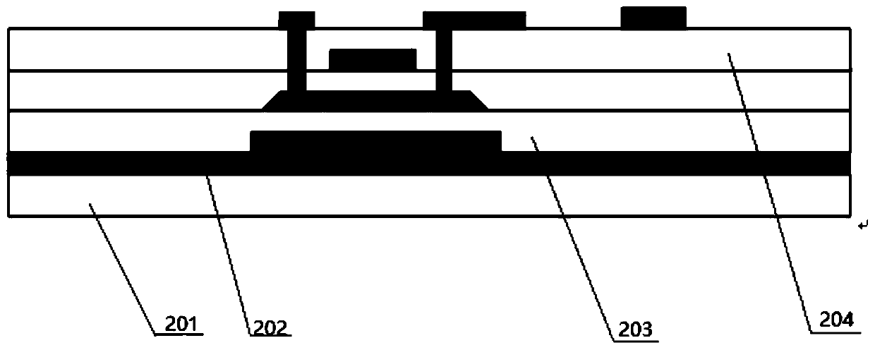
[0044] Such as figure 2 The partial schematic view of the traditional array substrate shown includes: a substrate 201, a PI layer 202, a thin film transistor layer 203 and a dielectric layer 204. When performing a curved LCD (liquid crystal display) process, the PI layer 202 of the first transistor is arranged on On the substrate 201, af...

Embodiment 2

[0054] An embodiment of the present invention also provides a display device. The display device includes the above-mentioned array substrate. The array substrate includes a substrate, and a PI layer, a protective layer, a thin film transistor layer and a layer stacked on the substrate. Dielectric layer; wherein, the PI layer is attached on the substrate;

[0055] The medium layer includes an inorganic medium layer and an organic medium layer stacked.

[0056] The material of the protective layer includes SiOx, and the thickness of the protective layer includes 0.2-0.3 μm.

[0057] The material of the inorganic medium layer includes at least SiNx, and the thickness range of the inorganic medium layer includes 0.1-0.3 μm.

[0058] The material of the organic medium layer includes polysilsesquioxane photosensitive resin, and the thickness range of the organic medium layer includes 0.8-1.2 μm.

[0059] In the embodiment of the present invention, the protective layer is used to ...

Embodiment 3

[0061] refer to Figure 6 , shows a flow chart of a method for preparing a film layer structure in an embodiment of the present invention.

[0062] Step 601, providing a substrate.

[0063] In this embodiment, the substrate is a glass substrate.

[0064] Step 602, attaching a PI layer on the substrate.

[0065] In this embodiment, the PI layer is made of a polyimide material layer, and the main chain of the PI molecule has a stable imide aromatic heterocyclic structure, and its stretchability can reach 200 MPa.

[0066] Step 603, forming a protection layer on the PI layer.

[0067] In the embodiment of the present invention, the PI layer that has been fabricated before is attached to the substrate, and a protective layer is formed on the PI layer by CVD. The material of the protective layer is SiOx, and a thickness of 0.2-0.3μm SiOx protective layer. The CVD (Chemical Vapor Deposition, chemical vapor deposition) method refers to introducing the vapor of the gaseous reacta...


PUM

PropertyMeasurementUnit
thicknessaaaaaaaaaa
thicknessaaaaaaaaaa
thicknessaaaaaaaaaa

Abstract

The invention provides an array substrate, a display device and a preparation method of the array substrate. The array substrate comprises a substrate, and a PI layer, a protection layer, a thin filmtransistor layer and a dielectric layer, which are attached to the substrate; and the dielectric layer comprises an inorganic dielectric layer and an organic dielectric layer which are arranged in a laminated manner. The protective layer is used for preventing the substrate from being influenced by water vapor and impurities during other processes; and meanwhile, when the laser is used for separating the glass, heat is isolated, laser energy is absorbed, and the influence of the laser on electrical characteristics of the P-type silicon in the transistor is avoided. The dielectric layer comprises an inorganic dielectric layer and an organic dielectric layer, and compared with a traditional dielectric layer which only comprises the inorganic dielectric layer and is thicker in inorganic dielectric layer, the embodiment of the invention reduces the thickness of the inorganic dielectric layer, adds one organic dielectric layer, improves the ductility and flatness of the dielectric layer, and can prevent the dielectric layer from being broken.

Description

technical field [0001] The present invention relates to the field of display technology, in particular to an array substrate, a display structure and a preparation method of the array substrate. Background technique [0002] At present, curved screen display has become mainstream. Compared with curved OLED, curved LCD has great advantages in cost, reliability, and service life. In the curved LCD process, the substrate is usually made on the Glass substrate. After the TFT and CF box alignment process is completed, the Glass on both sides is peeled off to expose the substrate engineering plastic for bending. However, this process often has the following disadvantages: [0003] 1. When laser stripping the Glass base, the laser energy is too high to irradiate P-Si (P-type silicon) and it is easy to cause abnormal electrical characteristics; [0004] 2. When bending, it is easy to cause the dielectric layer to break and then the SD metal wire to break, resulting in a large numbe...

Claims


Application Information

Patent Timeline
Patent Type & Authority Applications(China)
IPC IPC(8): H01L27/12H01L21/77G02F1/1362
CPCG02F1/1362H01L21/77H01L27/12
Inventor 刘弘方业周王凤国武新国郭志轩李凯田亮王海东马波杨越张东冯宇
Owner BOE TECH GRP CO LTD
Why Eureka
Try Eureka