Wafer polishing system for reducing defects in manufacturing of semiconductor devices

A semiconductor and device technology, applied in the field of wafer polishing systems, can solve the problems of inconvenience, poor polishing stability, inability to rise and fall, etc., and achieve the effects of convenient use and high polishing stability

Inactive Publication Date: 2018-06-05
王孝裕
View PDF1 Cites 0 Cited by
  • Summary
  • Abstract
  • Description
  • Claims
  • Application Information

AI Technical Summary

Problems solved by technology

[0004] Aiming at the deficiencies in the existing technology, the purpose of the present invention is to provide a wafer polishing system for reducing defects in the manufacture of semiconductor devices, so as to solve the problem that the existing technology cannot be raised and lowered when the equipment is polished, and it is inconvenient to use. And the problem of poor polishing stability

Method used


Image

  • Wafer polishing system for reducing defects in manufacturing of semiconductor devices
  • Wafer polishing system for reducing defects in manufacturing of semiconductor devices
  • Wafer polishing system for reducing defects in manufacturing of semiconductor devices

Examples


Embodiment Construction

[0022] In order to make the technical means, creative features, goals and effects achieved by the present invention easy to understand, the present invention will be further described below in conjunction with specific embodiments.

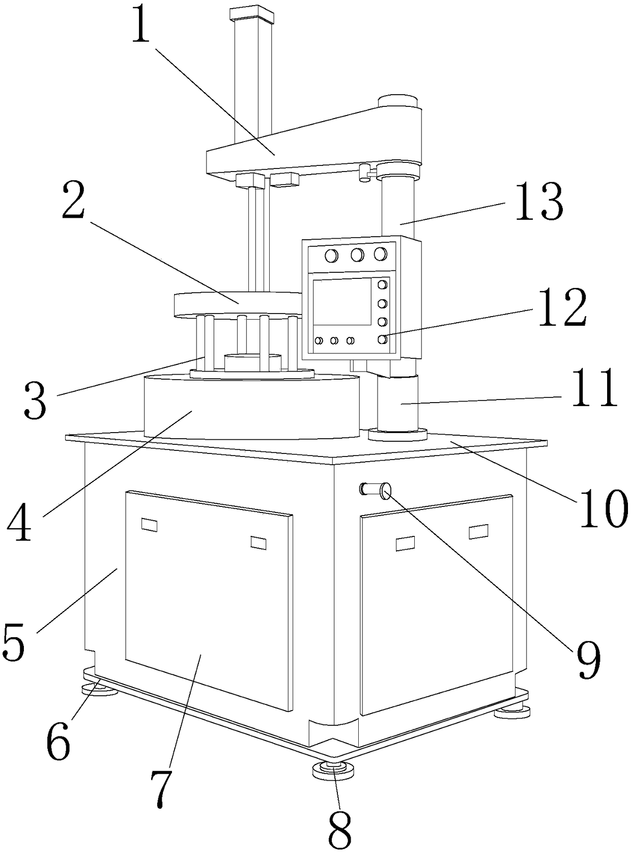
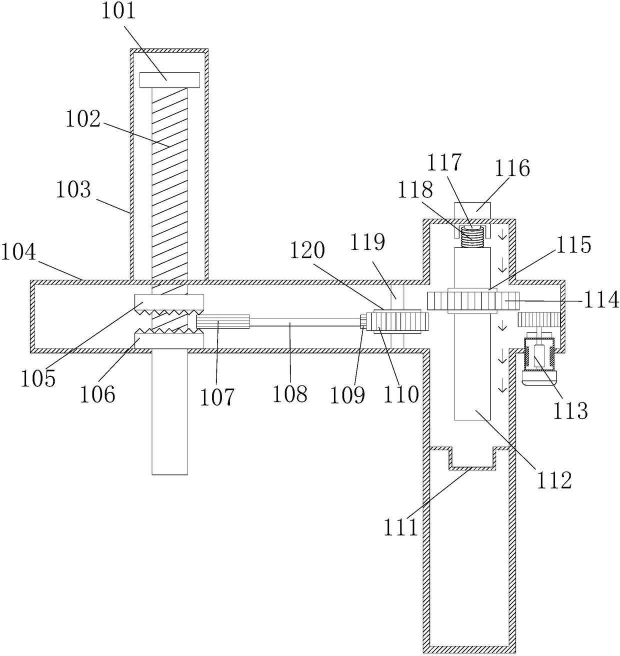
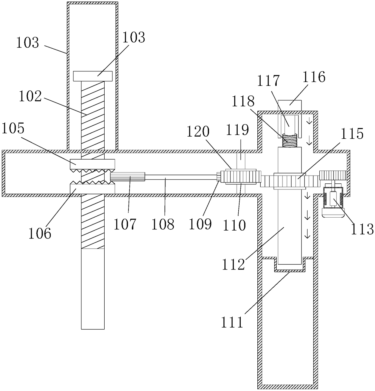
[0023] see Figure 1-Figure 5, the present invention provides a technical scheme of a wafer polishing system for reducing defects in the manufacture of semiconductor devices: its structure includes a lifting adjustment rod 1, a polishing wheel 2, a support rod 3, a polishing table 4, a machine base 5, a base plate 6, a maintenance Plate 7, supporting feet 8, plate locking device 9, workbench 10, rotating base 11, operation box 12, extension rod 13, the middle part of the base 5 is connected with the maintenance plate 7 by interference fit, and the maintenance plate 7 is a square structure with more than two parallel to each other, the base plate 6 and the workbench 10 are parallel to each other, the base plate 6 is welded vertically to the bottom ...


PUM


Abstract

The invention discloses a wafer polishing system for reducing defects in manufacturing of semiconductor devices. The wafer polishing system structurally comprises a lifting and debugging rod, two circular polishing wheels, a supporting rod, a polishing table, a seat, a base plate, more than two square maintaining plates, supporting legs, a plate locking device, a worktable, a rotatable base, an operation box and an lengthening rod, the middle of the seat is in interference fit with the maintaining plate, every two maintaining plates parallel to each other, the base plate is mutually parallel to the worktable and vertically welded with the lower portion of the seat, the worktable is vertically welded with the upper portion of the seat, the right lower portion of the lifting and debugging rod is in interference fit with the outer side of the lengthening rod, and the polishing wheels are vertically welded with the upper end and the lower end of the supporting rod. By the aid of the structure, the system is provided with the lifting and debugging rod, the system can rise and fall when being used for polishing, and the system is convenient to use and high in polishing stability.

Description

technical field [0001] The invention relates to a wafer polishing system for reducing defects in manufacturing semiconductor devices, belonging to the field of wafer polishing systems. Background technique [0002] A chemical mechanical polishing system is known as a system for polishing the surface of a substrate such as a semiconductor substrate. Typically, the system has a polishing table, a polishing disk attached to an upper surface of the polishing table, and a substrate holding mechanism. The polishing disc provides a polishing surface for polishing the substrate. The substrate holding mechanism presses the substrate to be polished against the polishing surface of the polishing disc, and at the same time supplies the slurry to the polishing surface, and rotates the polishing table and the substrate holding mechanism to make the relative movement between the polishing surface and the substrate surface for polishing. and planarize the substrate surface. [0003] The ...

Claims


Application Information

Patent Timeline
Patent Type & Authority Applications(China)
IPC IPC(8): B24B37/10B24B7/22B24B37/34B24B47/22
CPCB24B37/10B24B7/228B24B37/34B24B47/22
Inventor 王孝裕
Owner 王孝裕
Why Eureka
Try Eureka