Wafer back surface cleaning and drying device and wafer back surface cleaning and drying system and method

A technology for drying devices and wafers, applied in electrical components, semiconductor/solid-state device manufacturing, circuits, etc., can solve problems such as unsatisfactory cleaning and drying effects, and the cleaning and drying methods cannot cover the entire or overlap the back of the wafer, etc. Achieve the effect of improving cleaning and drying effect, effective cleaning and drying, and simple device structure

Inactive Publication Date: 2018-06-05
BEIJING SEMICON EQUIP INST THE 45TH RES INST OF CETC
View PDF8 Cites 5 Cited by
  • Summary
  • Abstract
  • Description
  • Claims
  • Application Information

AI Technical Summary

Problems solved by technology

[0003] The object of the present invention is to provide a wafer backside cleaning and drying device, wafer backside cleaning and drying system and method, to solve the problem that the cleaning and drying methods in the prior art cannot cover the entire or overlapped backside of the wafer, resulting in cleaning Technical problems with unsatisfactory drying effect

Method used


Image

  • Wafer back surface cleaning and drying device and wafer back surface cleaning and drying system and method
  • Wafer back surface cleaning and drying device and wafer back surface cleaning and drying system and method
  • Wafer back surface cleaning and drying device and wafer back surface cleaning and drying system and method

Examples


Embodiment 1

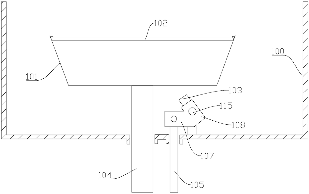
[0031] see figure 1 As shown, Embodiment 1 of the present invention provides a wafer backside cleaning and drying device including a wafer clamping device 101, a first driving device and a spraying mechanism. The wafer clamping device 101 is used to carry a wafer 102; the first driving device The device is used to drive the wafer clamping device 101 to rotate; the spraying mechanism is used to clean and dry the backside of the wafer; the spraying mechanism includes a nozzle 103, and the spraying path of the nozzle 103 to the backside of the wafer gradually changes from the center of the backside of the wafer Move to the edge of the back side of the wafer. In this embodiment, no improvement is made to the wafer clamping device 101, which is a prior art. Therefore, the description of the wafer clamping device 101 involved in the following embodiments is only used to more fully describe the present invention technical solutions and more clearly embody the features of the present...

Embodiment 2

[0046] The second embodiment also provides a cleaning and drying device for the back of the wafer. The cleaning and drying device for the back of the wafer in this embodiment describes another implementation of the injection mechanism. In addition to the technical solution of the first embodiment It also belongs to the second embodiment and will not be described again.

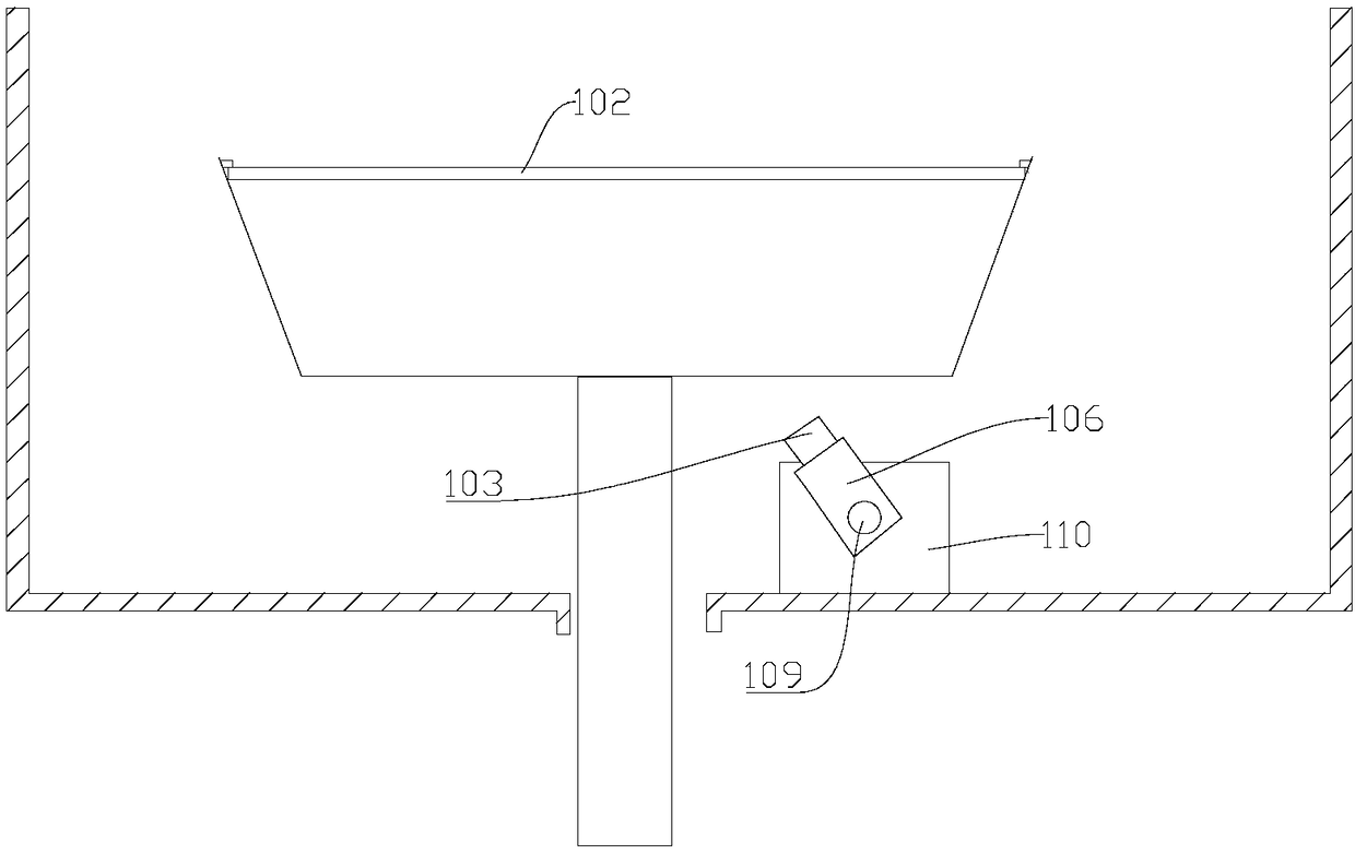
[0047] see figure 2 As shown, in this embodiment, the injection mechanism includes a movable block 106 and a nozzle 103; the nozzle 103 is installed on the movable block 106, and the movable block 106 is installed on the second rotating shaft 109, and the second rotating shaft 109 is connected with the fourth rotating shaft through a gear or a synchronous belt. The driving device is driven, and the fourth driving device can be a motor 110; the motor rotates so that the angle of the second rotating shaft 109 is changed, so that the movable block 106 is deflected, and the movement of the movable block 106 drive...

Embodiment 3

[0049] The third embodiment also provides a cleaning and drying device for the back of the wafer. The cleaning and drying device for the back of the wafer in this embodiment describes another implementation of the wafer clamping device 101. Other embodiments The technical solution of Embodiment 1 or Embodiment 2 also belongs to Embodiment 3 and will not be described again.

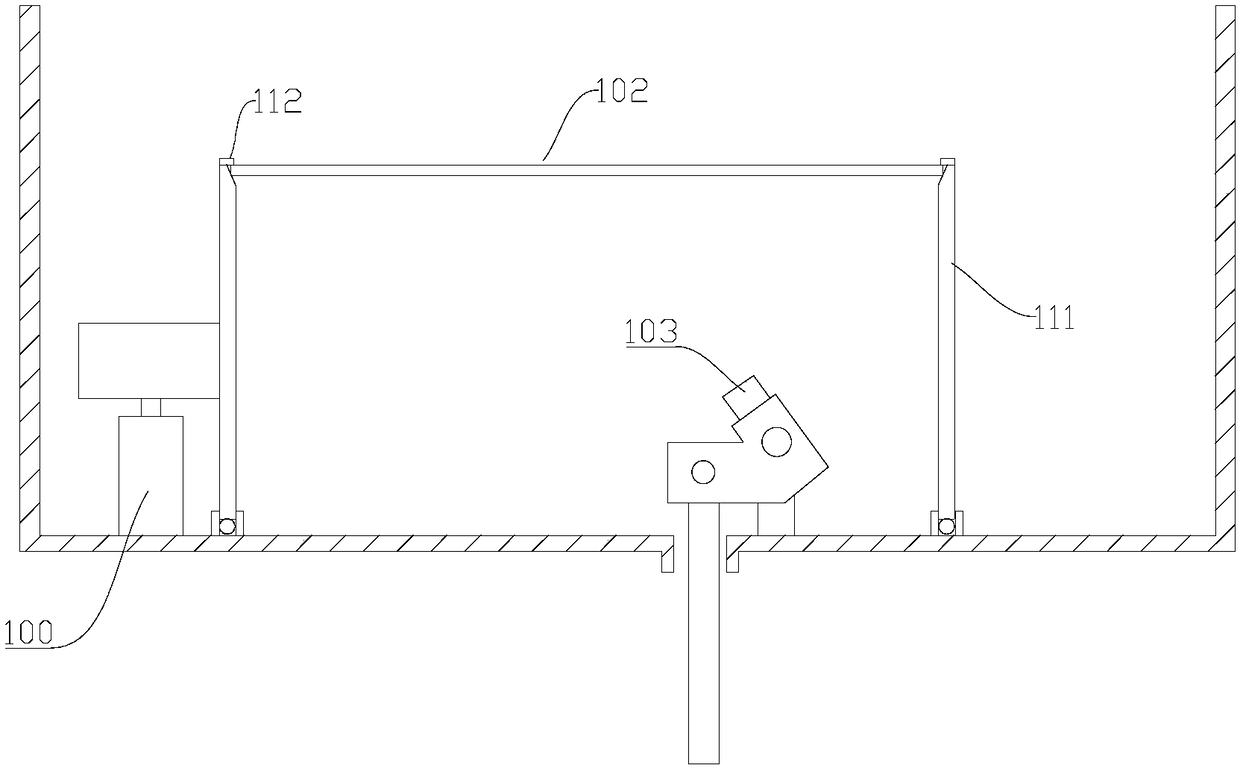
[0050] see image 3 As shown, in this embodiment, the wafer clamping device 101 includes a barrel ring 111 and a plurality of fixing clips 112, and the plurality of fixing clips 112 are evenly distributed along the circumference of the barrel ring 111; The outer third driving device 113 is driven, and the third driving device 113 drives the bucket rim 111 to rotate through gear transmission. The third driving device 113 is a motor 110. The injection mechanism is located within the circle of the barrel circle 111 . The bottom of the barrel ring is limited in the limiting groove, and there are balls betwe...


PUM


Abstract

The invention relates to the technical field of wafer back surface cleaning equipment, and particularly relates to a wafer back surface cleaning and drying device and a wafer back surface cleaning anddrying system and method. The wafer back surface cleaning and drying device comprises a wafer clamping device, a first driving device and a spraying mechanism, wherein the wafer clamping device is used for carrying a wafer; the first driving device is used for driving the wafer clamping device to rotate; the spraying mechanism is used for cleaning and drying the back surface of the wafer; and thespraying mechanism comprises a nozzle, and the spraying path of the nozzle for the back surface of the wafer gradually moves from the center of the back surface of the wafer to the edge of the back surface of the wafer. The wafer back surface cleaning and drying system comprises the wafer back surface cleaning and drying device. According to the invention, the back surface of the whole wafer canbe cleaned and dried, the device is simple in structure, and the overlapping of cleaning and drying areas can be realized according to requirements, thereby achieving effective cleaning and drying forthe back surface of the wafer, and improving the cleaning and drying effect of the back surface of the wafer.

Description

technical field [0001] The invention relates to the technical field of wafer back cleaning equipment, in particular to a wafer back cleaning and drying device, a wafer back cleaning and drying system and method. Background technique [0002] With the continuous shrinking of the critical dimensions of the semiconductor device process, the requirements for the wafer process are more stringent, and the requirements for the cleaning and drying effect of the back of the wafer are also getting higher and higher. At present, in the process of wafer processing, when the back of the wafer is processed, multiple fixed nozzles are used for fixed-point spraying, that is, the nozzles spray the fixed position of the back of the wafer to achieve cleaning. For the purpose of drying, the structure of the device adopting this cleaning and drying method is complicated, and it cannot cover the entire or overlapped backside of the wafer, resulting in unsatisfactory cleaning and drying effects. ...

Claims


Application Information

Patent Timeline
IPC IPC(8): H01L21/67H01L21/02
CPCH01L21/02041H01L21/67034
Inventor 舒福璋史霄佀海燕田知玲陶利权
Owner BEIJING SEMICON EQUIP INST THE 45TH RES INST OF CETC
Why Eureka
Try Eureka