Universal host for RG or RGB emission in organic light emitting devices

a light emitting device and universal host technology, applied in the direction of discharge tube luminescnet screens, discharge tube/lamp details, electric discharge lamps, etc., can solve the problems of large reduction of optical power of white oled, accelerate degradation and shorten the life of the device, etc., to achieve easy color tuning, good color chromaticity, and maintain device efficiency

Inactive Publication Date: 2007-05-22
THE UNITED STATES OF AMERICA AS REPRESENTED BY THE SECRETARY OF THE NAVY
View PDF13 Cites 22 Cited by
  • Summary
  • Abstract
  • Description
  • Claims
  • Application Information

AI Technical Summary

Benefits of technology

[0010]RGB emission can be achieved using universal host / dopant systems as the emitting layer in OLED pixels. This approach allows the display to be easily color tuned by modifying only one element of the device structure, the dopant. The advantage of combining two mechanisms, energy transfer and direct carrier recombination, allows us to use common host materials for different dopants while still maintaining device efficiency and good color chromaticity. In addition, this method minimizes the number of processing steps thus simplifying the device structures and reducing the risk of cross contamination. A new feature of this invention is the use of a universal host for RGB dopants to achieve fall color displays using OLEDs. It is the object of this invention to provide an approach to simplify OLED structures and minimize the number of materials used to achieve RGB color emission. A full-color display utilizing a universal host, as described in this invention, does not rely solely on good spectral overlap between host emission and guest absorption (energy transfer) to achieve red emission. The present invention details several possibilities for the usefulness of this concept. A single universal host can be used for R, G, and B dopants (see FIG. 1(a)). Additionally, if the universal host has blue emissive properties, it can be used undoped to further reduce the number of materials. Likewise, if the universal host has carrier transport properties, the need for additional hole or electron transport materials is eliminated (see FIGS. 1(b) and 1(c)). Another example utilizes the emission properties of either or both of the carrier transport layers to obtain one or more of the RGB pixels, which again reduces the number of materials used in the devices. A specific example of this last method is described in detail below.

Problems solved by technology

Developing efficient and economical methods to manufacture RGB patterned pixels is one of the main issues concerning the realization of full-color flat panel displays.
This technique results in a large reduction of the optical power from the white OLED.
Thus the color-filtered OLEDs must be operated at high brightness / current density, which may accelerate degradation and shorten the lifetime of the device.
A major challenge of this method is the difficulty of finding a red fluorescent material with a high absorption coefficient in the blue wavelength region and having a high fluorescence in the red wavelength region.
This method also results in reduced device efficiency during the color conversion process.
The use of several different types of material components during device fabrication may increase the risk for cross-contamination and would bring about a more complicated process for device fabrication.

Method used


Image

  • Universal host for RG or RGB emission in organic light emitting devices
  • Universal host for RG or RGB emission in organic light emitting devices

Examples


example 1

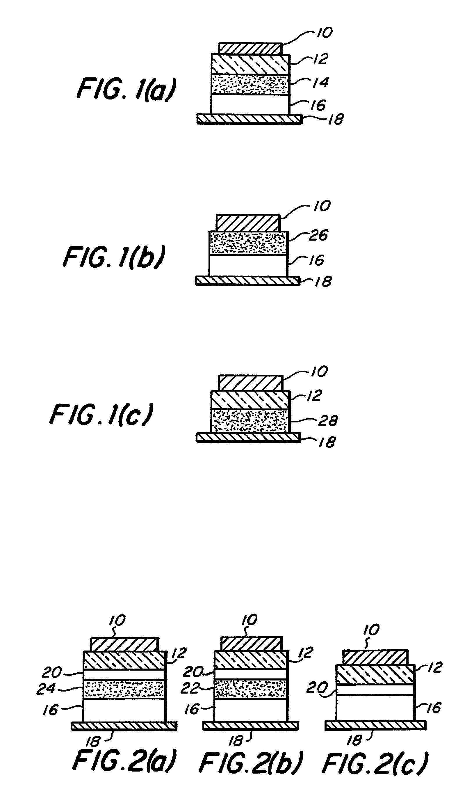
[0021]RGB emission was achieved with a universal host used for RG OLED pixels fabricated with similar device structures, with the exception of the emitting species. The blue emissive properties of the hole transport material, 4,4-bis(1-naphthylphenylamino)biphenyl (NPB) were utilized for the B OLED pixel (see FIG. 1(c)).

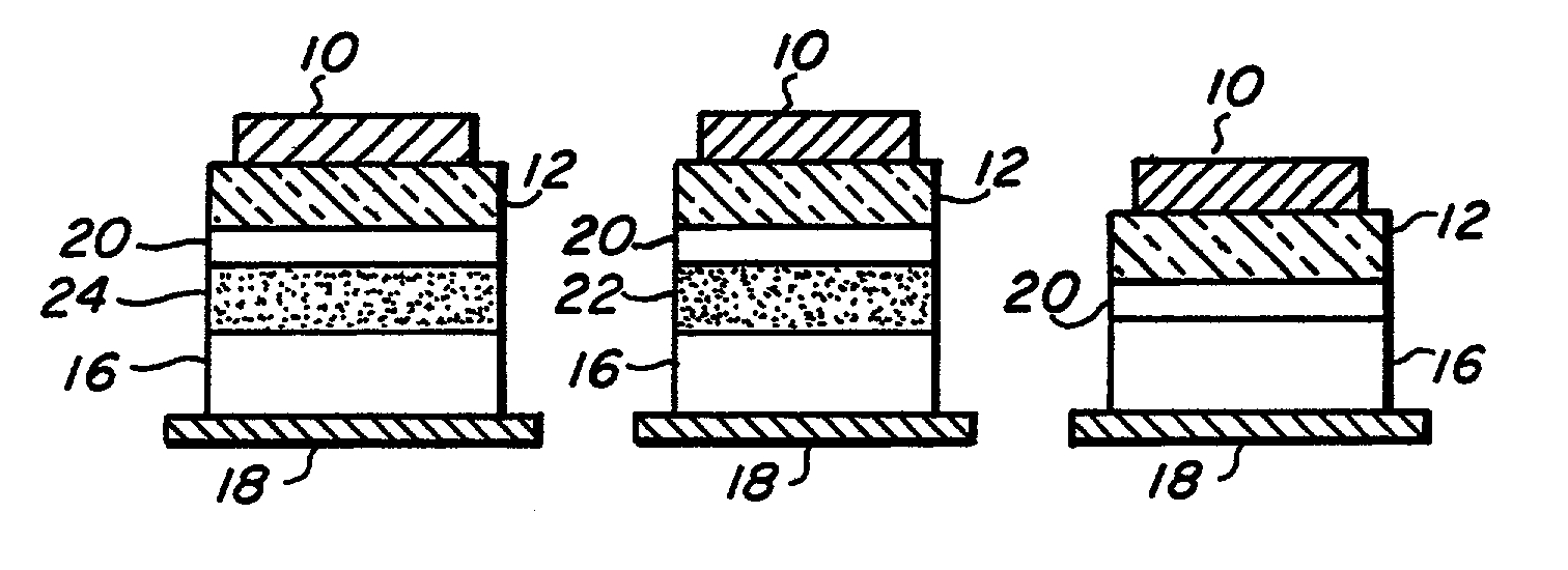
[0022]OLED RGB device structures and organic materials used in this example are shown in FIGS. 2(a) through 2(c). All materials were vacuum deposited inside a chamber under a base pressure of approximately 10−7 Torr. All devices contain of a glass substrate coated with a transparent anode material, here indium tin oxide (ITO). In addition, the hole transporting layer in all devices is NPB. The hole blocking layer is bathocuproine (2,9-dimethyl-4,7-diphenyl-1,10-phenanthroline)(BC) in all three devices. Lastly, all devices utilized 5,5′-bis(dimesityl-boryl)-2,2′-bithiophene (BMB-2T), as the electron transport layer.

[0023]For the red and green OLED devices (FIGS. 2(a) ...

example 2

[0024]We have also postulated that RGB emission can be readily achieved where the universal host used for RG OLED pixels is fabricated with similar device structures as described above in Example 1. The blue emissive properties of the universal host can be utilized for the B OLED pixel. The devices consist of glass substrate coated with indium tin oxide (ITO), a transparent anode material. For all of the devices, the hole transporting layers are NPB. The electron transport layers are composed of separate layers of o-TTA and 5,5′-bis(dimesitylboryl)-2,2′-bithiophene (BMB-2T). The o-TTA layer also functions to allow for generation and transmittance of blue light because it serves to prevent the formation of an exciplex between the NPB and BMB-2T layers (See Shirota, J MAT Chem., 10, 1–25 (2000), herein incorporated by reference). For the green and red devices, a composite film of the universal host material, BMB-2T, and dopant, would be inserted between the o-TTA and BMB-2T layers to ...


PUM


Abstract

The present invention describes the use of red, green and, if necessary, blue dopants dispersed in a universal host material as the active emitting layer in OLEDs. The universal host is transparent in the visible region, and may be emissive in the blue region when used as the blue emitting species or possesses carrier transport properties. By dispersing the dopants in the universal host, efficient energy transfer from host to guest and/or direct carrier recombination on the dopant takes place resulting in bright red, green or blue emission, depending on the dopant. The resulting spectra are characteristic of the guest molecules.

Description

RELATED APPLICATIONS[0001]This is a Non-provisional Application relating to a previously filed Provisional Application, PTO No. 60 / 253,717, filed on Nov. 29, 2000.BACKGROUND OF THE INVENTION[0002]1. Field of the Invention[0003]This invention relates to colored light emission in light emitting device structures for use in a variety of apparatuses.[0004]2. Description of the Background Art[0005]Organic light emitting devices (OLEDs) are an emerging technology that may soon replace liquid crystal displays (LCDs) in flat panel display applications due to their desirable characteristics including self-emissive high brightness, wide viewing angles, light-weight, and low power consumption. Recently, Sony previewed a prototype of an OLED-based display that is slightly thicker than a credit card and announced production to start in 2003. A display is made up of many tiny individual pixels (picture elements) where, an OLED represents one pixel. In a full-color display, each pixel contains one...

Claims


Application Information

Patent Timeline
Patent Type & Authority Patents(United States)
IPC IPC(8): H01J1/63H01L51/30H01L51/50
CPCH01L51/008H01L51/5012H01L51/005H10K85/60H10K85/322H10K50/11
Inventor KAFAFI, ZAKYA H.PICCIOLO, LISA C.MURATA, HIDEYUKI
Owner THE UNITED STATES OF AMERICA AS REPRESENTED BY THE SECRETARY OF THE NAVY
Why Eureka
Try Eureka