Pull-up circuit for IO circuit
A circuit and power supply technology, applied in the direction of logic circuit, logic circuit coupling/interface using field effect transistor, logic circuit interface device, etc., can solve the problems affecting the normal output of IO circuit, and achieve the effect of preventing backflow
- Summary
- Abstract
- Description
- Claims
- Application Information
AI Technical Summary
Problems solved by technology
Method used
Image
Examples
Embodiment Construction
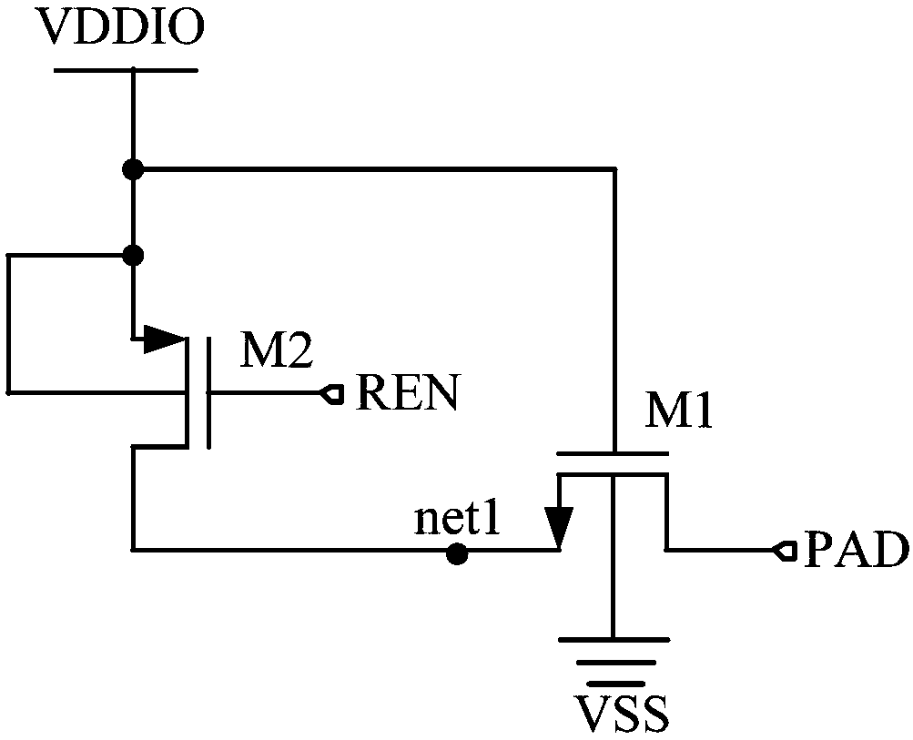
[0030] Those skilled in the art understand that the existing pull-up circuits for IO circuits generally adopt figure 1 The circuit configuration shown. exist figure 1 In the shown circuit structure, M1 is an NMOS transistor, M2 is a PMOS transistor, REN is a pull-up control signal, net1 is node 1 and is used to connect the source of the NMOS transistor M1 and the drain of the PMOS transistor M2. according to figure 1 The circuit structure shown, when in fail-safe mode (for example, the voltage value VDDIO of the IO power supply is suddenly powered off, while the voltage value of the IO port signal is logic high level), or the input signal voltage value of the IO port is higher than normal When the voltage value of the IO power supply under operation is VDDIO, even if the NMOS transistor M1 is turned on, the voltage value of the net1 is still smaller than the IO power supply voltage by at least the threshold voltage of M1, ensuring that there will be no transition from the IO...
PUM
 Abstract
Description
Claims
Application Information


