Array substrate and preparation method thereof
An array substrate and base substrate technology, which is applied in the field of array substrates and their preparation, can solve the problem that the pixel electrode layer 14' is prone to breakage and the like, and achieve the effect of avoiding pollution
- Summary
- Abstract
- Description
- Claims
- Application Information
AI Technical Summary
Problems solved by technology
Method used
Image

Examples
Embodiment 1
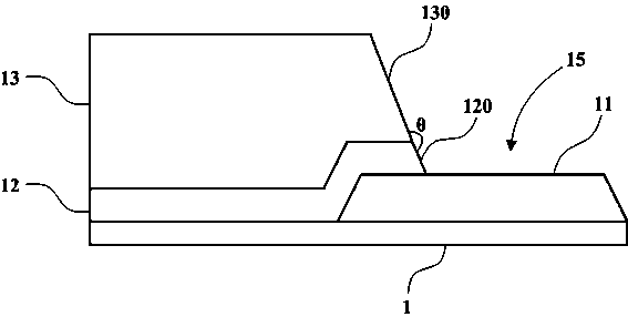
[0049] please refer again Figure 8 As shown, corresponding to Embodiment 1 of the present invention, Embodiment 2 of the present invention provides a method for preparing an array substrate, including:
[0050] providing a base substrate;
[0051] sequentially forming a metal layer, a passivation layer and a flat layer on the base substrate;
[0052] Etching the flat layer and the passivation layer on the metal layer in two steps to form a contact hole, so that the metal layer is at least partially exposed to the contact hole, and the contact hole is at the passivation layer The hole wall is in the same plane or forms an obtuse angle with the hole wall at the flat layer;
[0053] A continuous pixel electrode layer is formed at the flat layer and the contact hole, and the pixel electrode layer is connected to the metal layer.
[0054] Specifically, in this embodiment, the etching of the flat layer and the passivation layer on the metal layer is divided into two steps, where...
PUM
 Abstract
Description
Claims
Application Information
 - Generate Ideas
- Intellectual Property
- Life Sciences
- Materials
- Tech Scout
- Unparalleled Data Quality
- Higher Quality Content
- 60% Fewer Hallucinations
Browse by: Latest US Patents, China's latest patents, Technical Efficacy Thesaurus, Application Domain, Technology Topic, Popular Technical Reports.
© 2025 PatSnap. All rights reserved.Legal|Privacy policy|Modern Slavery Act Transparency Statement|Sitemap|About US| Contact US: help@patsnap.com