OLED display panel and manufacturing method thereof

A manufacturing method and display panel technology, applied in semiconductor/solid-state device manufacturing, semiconductor devices, electrical components, etc., can solve problems such as rising costs, complicated manufacturing process, short circuit, etc., and achieve the effect of cost saving and process simplification

Active Publication Date: 2020-08-28
TCL CHINA STAR OPTOELECTRONICS TECH CO LTD
View PDF4 Cites 0 Cited by
  • Summary
  • Abstract
  • Description
  • Claims
  • Application Information

AI Technical Summary

Problems solved by technology

Usually in the 2in1 pixel structure, the anodes connected to the two thin film transistors are separated in the middle (air gap), but this method is very easy to cause the risk of short circuit between the two anodes, thereby reducing the display quality
In addition, after the two anodes are fabricated, in order to meet the requirements of flatness and electrical insulation, a passivation layer is usually required to be fabricated on the two anodes before the pixel defining layer with pixel defining holes, which complicates the fabrication process. , the cost rises

Method used


Image

  • OLED display panel and manufacturing method thereof
  • OLED display panel and manufacturing method thereof
  • OLED display panel and manufacturing method thereof

Examples


Embodiment approach

[0039] Here, the manufacturing method of the thin film transistor according to the embodiment of the present invention is realized through steps 1 to 5, and such a method of manufacturing a thin film transistor is only one embodiment of the present invention, and the manufacturing method of the thin film transistor of the present invention does not limited to this.

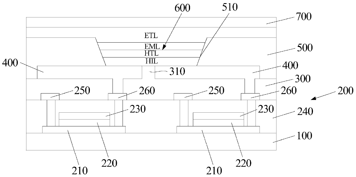
[0040] Next, refer to Figure 2F , on the second insulating layer 240 , the source electrode 250 and the drain electrode 260 , a planar layer 300 and spacer pillars 310 protruding upward from the planar layer 300 are formed. Here, the flat layer 300 and the spacer columns 310 can be formed simultaneously by using a half-tone mask to perform a yellow light process, thereby simplifying the process and reducing the cost.

[0041] Next, refer to Figure 2G Anodes 400 located on both sides of the spacer column 310 are formed on the planar layer 300 , and each anode 400 penetrates the planar layer 300 to be connected ...


PUM


Abstract

The present invention provides an OLED display panel, which comprises: a substrate; at least two thin film transistors arranged at intervals on the substrate; a flat layer arranged on the at least two thin film transistors; at least two anodes arranged at intervals On the planar layer, the anode penetrates the planar layer to connect with the corresponding thin film transistor; the spacer column is arranged in the space between the anodes; the pixel definition layer is arranged on the planar layer and have a pixel-defining hole exposing the spacer column and the at least two anodes; the OLED functional layer is disposed on the exposed spacer column and the at least two anodes; the cathode is disposed on the OLED functional layer . The invention also discloses a manufacturing method of the OLED display panel. The present invention forms spacer columns between adjacent anodes, thereby ensuring that the adjacent anodes are electrically insulated from each other while maintaining the interval between adjacent anodes, so that the display quality will not be affected.

Description

technical field [0001] The invention belongs to the technical field of organic display, and in particular relates to an OLED display panel and a manufacturing method thereof. Background technique [0002] In recent years, organic light-emitting diode (Organic Light-Emitting Diode, OLED) display panel has become a very popular emerging flat display panel product at home and abroad, because OLED display panel has self-illumination, wide viewing angle, short response time, high luminous efficiency, It has the characteristics of wide color gamut, thin thickness, large-size and flexible display panel and simple manufacturing process, and it also has the potential of low cost. [0003] One of the existing methods for manufacturing high-resolution OLED display panels is to use a 2in1 pixel structure, that is, two thin film transistors share a pixel to define the OLED functional layer in the hole, which can improve the printing accuracy. Usually, in the 2in1 pixel structure, the an...

Claims


Application Information

Patent Timeline
Patent Type & Authority Patents(China)
IPC IPC(8): H01L27/32H01L51/50H01L51/56
CPCH10K59/00H10K59/12H10K50/15H10K71/00
Inventor 林碧芬
Owner TCL CHINA STAR OPTOELECTRONICS TECH CO LTD
Why Eureka
Try Eureka