Eureka AIR delivers breakthrough ideas for toughest innovation challenges, trusted by R&D personnel around the world.

OLED functional layer ink jet printing preparation method and mask plate thereof

A technology of inkjet printing and mask plate, which is applied in semiconductor/solid-state device manufacturing, electrical components, electric solid-state devices, etc., can solve problems such as cumbersome process and quality influence of pixel electrodes, and achieve the effect of improving quality and reducing weight

Active Publication Date: 2018-06-19
TCL CHINA STAR OPTOELECTRONICS TECH CO LTD
View PDF7 Cites 3 Cited by
  • Summary
  • Abstract
  • Description
  • Claims
  • Application Information

AI Technical Summary

Problems solved by technology

However, the process of making pixel banks is quite cumbersome, and pixel banks have a great impact on the quality of pixel electrodes

Method used


Image

  • OLED functional layer ink jet printing preparation method and mask plate thereof
  • OLED functional layer ink jet printing preparation method and mask plate thereof
  • OLED functional layer ink jet printing preparation method and mask plate thereof

Examples


Embodiment Construction

[0025] The following are preferred embodiments of the present invention. It should be pointed out that for those skilled in the art, without departing from the principle of the present invention, some improvements and modifications can also be made, and these improvements and modifications are also considered as the present invention. protection scope of the invention.

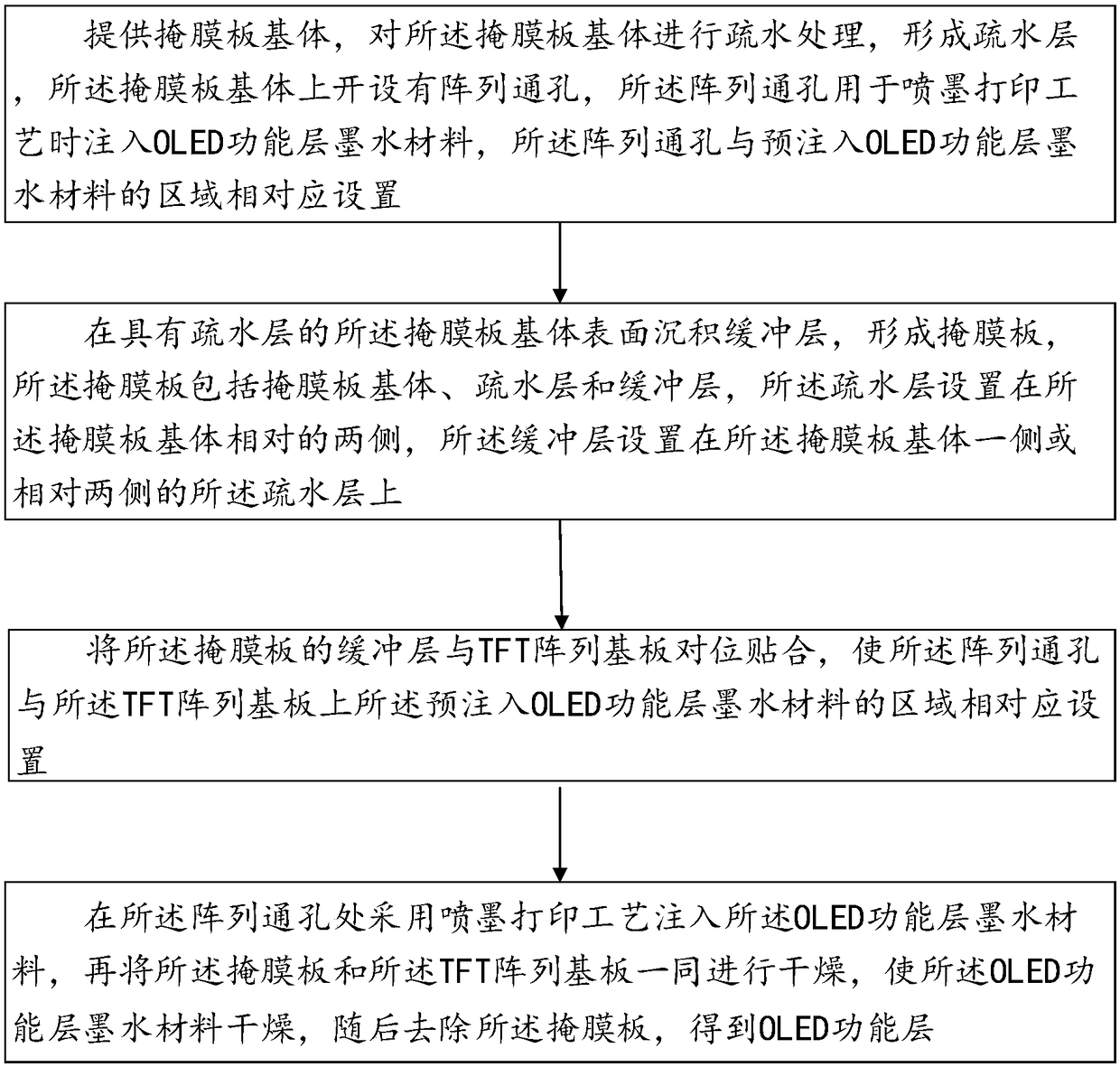
[0026] see Figure 1-Figure 3 , the first aspect of the present invention provides an OLED functional layer inkjet printing preparation method, comprising the following steps:

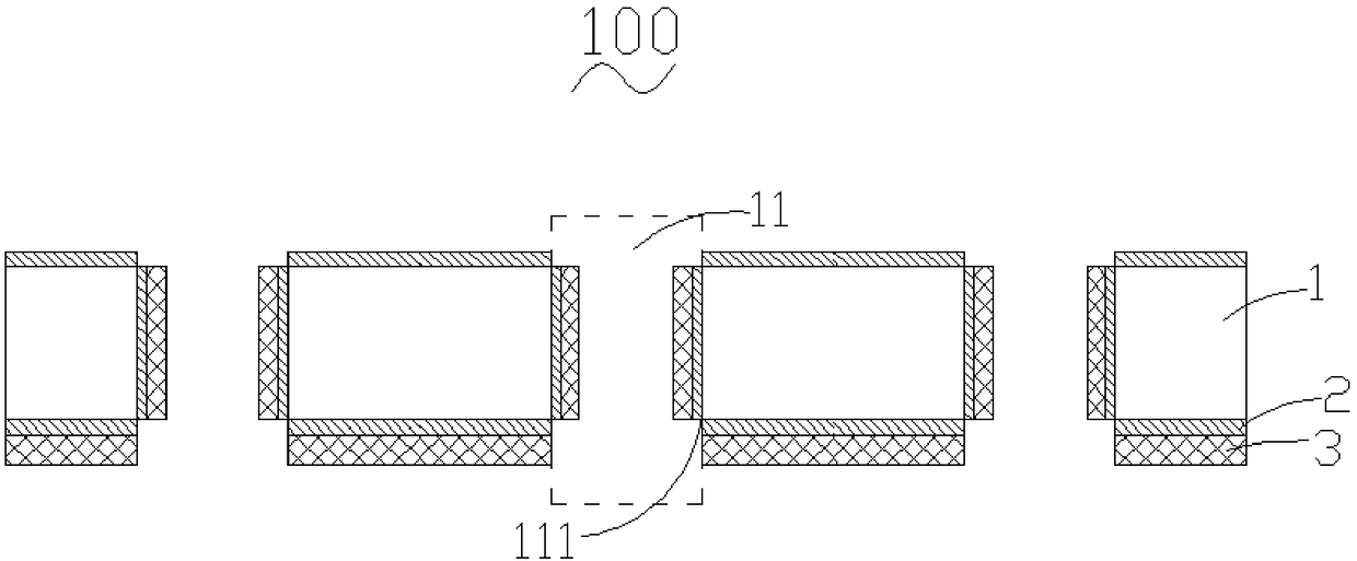
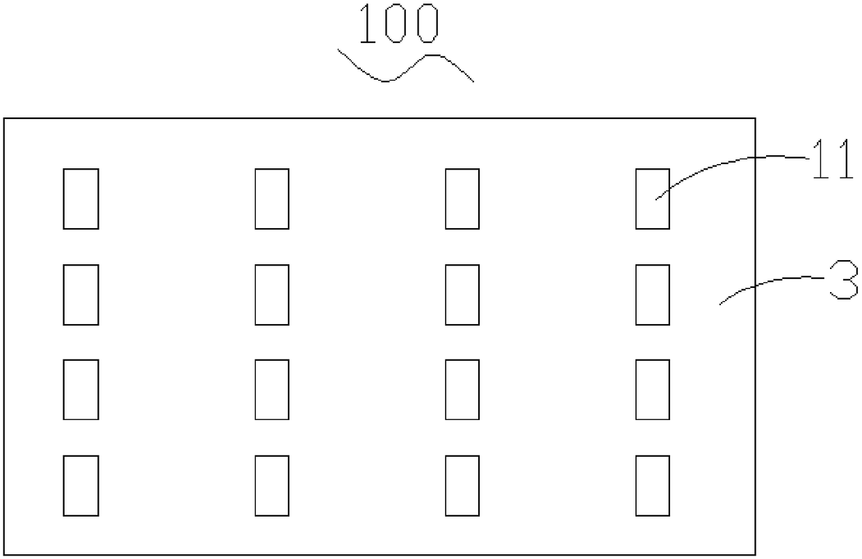
[0027] Step 1: Provide a mask base 1, perform hydrophobic treatment on the mask base 1 to form a hydrophobic layer 2, the mask base 1 is provided with an array of through holes 11, and the array through holes 11 are used for The OLED functional layer ink material is injected during the inkjet printing process, and the array through hole 11 is set corresponding to the area where the OLED functional layer ink material is pre-injected; ...


PUM

PropertyMeasurementUnit
Thicknessaaaaaaaaaa
Thicknessaaaaaaaaaa

Abstract

The invention provides an OLED functional layer ink jet printing preparation method. The method comprises the steps that a mask plate substrate is provided, hydrophobic treatment is carried out on themask plate substrate to form a hydrophobic layer; a buffer layer is deposited on the surface of the mask plate substrate with the hydrophobic layer to form the mask plate; the buffer layer of the mask plate is aligned with a TFT array substrate, so that mask plate array through holes are corresponding to a region pre-injected with an OLED functional layer ink material on the TFT array substrate;an ink jet printing process is used in the array through holes in the mask plate; an OLED HIL functional layer ink material is injected; the mask plate and the TFT array substrate are dried together to dry the ink of an OLED functional layer; and the mask plate is removed to acquire the OLED functional layer. The ink jet printing method is used for the mask plate with the hydrophobic layer and thebuffer layer on the surface to prepare the OLED functional layer. The preparation process of the pixel bank is omitted. The production process is greatly simplified. The production cost is reduced. The production efficiency and the OLED quality are improved.

Description

technical field [0001] The invention belongs to the technical field of OLED panel preparation, and in particular relates to an inkjet printing preparation method of an OLED functional layer and a mask plate thereof. Background technique [0002] Due to its excellent performance, OLED has become an emerging and popular flat panel display device. At present, inkjet printing technology is mainly used to realize full-color OLED. In the inkjet printing technology, in order to make the printed liquid material form better, it is necessary to prepare a pixel bank around the pixel electrode, and then inject the OLED functional layer ink material into the pixel bank area. However, the process of making the pixel bank is quite cumbersome, and the pixel bank has a great impact on the quality of the pixel electrode. Therefore, it is urgent to find a new method to prepare pixel electrodes. Contents of the invention [0003] The purpose of the present invention is to provide a prepara...

Claims


Application Information

Patent Timeline
IPC IPC(8): H01L51/56H01L51/00
CPCH10K71/135H10K71/00
Inventor 邓联谱
Owner TCL CHINA STAR OPTOELECTRONICS TECH CO LTD
Why Eureka
Eureka Blog
Learn More