A Heterojunction Potential Controlled Insulated Gate Bipolar Transistor
A heterojunction and insulated gate technology, which is applied in the direction of circuits, electrical components, semiconductor devices, etc., to achieve the effect of optimizing the compromise relationship, improving the reliability of large currents, and suppressing the NDR phenomenon
- Summary
- Abstract
- Description
- Claims
- Application Information
AI Technical Summary
Problems solved by technology
Method used
Image

Examples
Embodiment 1
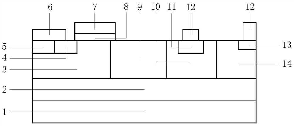
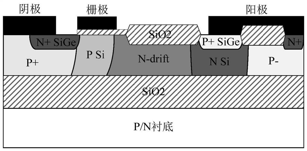
[0041] like figure 1 As shown, a heterojunction potential-controlled insulated gate bipolar transistor is characterized in that it includes an SOI substrate, a drift region, an anode region, a cathode region and a gate region.
[0042] The SOI substrate includes a substrate layer 1, a dielectric layer 2 and a top silicon layer.
[0043] The substrate layer 1 is a P-type or N-type doped silicon material; its typical impurity concentration is the 14th power;
[0044] The dielectric layer 2 covers the substrate layer 1, and the dielectric layer 2 is made of silicon dioxide. Determined according to the withstand voltage requirements of the designed device, the typical thickness is 0.5 μm to 5 μm.
[0045] The top layer of silicon covers the dielectric layer 2 , and the top layer of silicon is P-type or N-type doped silicon material.
[0046] A heterojunction potential-controlled insulated-gate bipolar transistor conduction functional region is formed in the top silicon layer. ...
Embodiment 2
[0064] like figure 2 As shown, a heterojunction potential-controlled insulated gate bipolar transistor is characterized in that it includes an SOI substrate, a drift region, an anode region, a cathode region and a gate region.
[0065] The SOI substrate includes a substrate layer 1, a dielectric layer 2 and a top silicon layer.
[0066] The substrate layer 1 is a P-type or N-type doped silicon material; its typical impurity concentration is the 14th power;
[0067] The dielectric layer 2 covers the substrate layer 1, and the dielectric layer 2 is made of silicon dioxide. Determined according to the withstand voltage requirements of the designed device, the typical thickness is 0.5 μm to 5 μm.
[0068] The top layer of silicon covers the dielectric layer 2 , and the top layer of silicon is P-type or N-type doped silicon material.
[0069] A heterojunction potential-controlled insulated-gate bipolar transistor conduction functional region is formed in the top silicon layer. ...
Embodiment 3
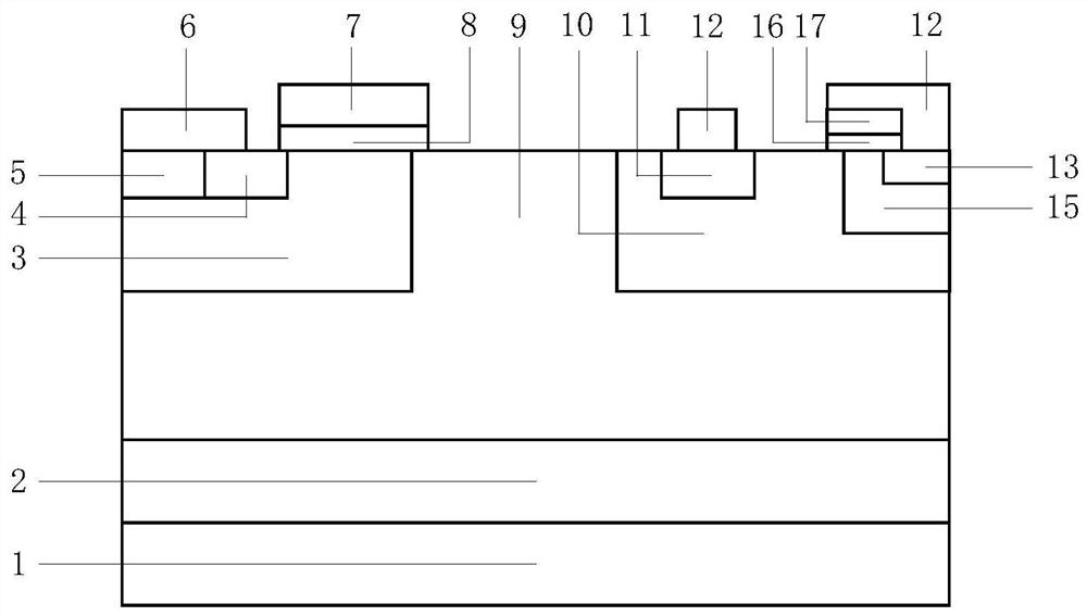
[0087] like image 3 As shown, a heterojunction potential-controlled insulated gate bipolar transistor is characterized in that it includes an SOI substrate, a drift region, an anode region, a cathode region and a gate region.
[0088] The SOI substrate includes a substrate layer 1, a dielectric layer 2 and a top silicon layer.
[0089] The substrate layer 1 is a P-type or N-type doped silicon material; its typical impurity concentration is the 14th power;
[0090] The dielectric layer 2 covers the substrate layer 1, and the dielectric layer 2 is made of silicon dioxide. Determined according to the withstand voltage requirements of the designed device, the typical thickness is 0.5 μm to 5 μm.
[0091] The top layer of silicon covers the dielectric layer 2 , and the top layer of silicon is P-type or N-type doped silicon material.
[0092] A heterojunction potential-controlled insulated-gate bipolar transistor conduction functional region is formed in the top silicon layer. ...
PUM
| Property | Measurement | Unit |
|---|---|---|
| thickness | aaaaa | aaaaa |
| thickness | aaaaa | aaaaa |
| thickness | aaaaa | aaaaa |
Abstract
Description
Claims
Application Information
 - R&D
- Intellectual Property
- Life Sciences
- Materials
- Tech Scout
- Unparalleled Data Quality
- Higher Quality Content
- 60% Fewer Hallucinations
Browse by: Latest US Patents, China's latest patents, Technical Efficacy Thesaurus, Application Domain, Technology Topic, Popular Technical Reports.
© 2025 PatSnap. All rights reserved.Legal|Privacy policy|Modern Slavery Act Transparency Statement|Sitemap|About US| Contact US: help@patsnap.com