Check patentability & draft patents in minutes with Patsnap Eureka AI!

Pixel structure

A technology of pixel structure and pixel electrode, applied in the field of pixel structure, can solve the problems of increased distance between gate and semiconductor layer, poor subcritical swing, too small turn-on current, etc., to achieve improved subcritical swing, increased number of channels, Turn on the effect of increasing the current

Active Publication Date: 2018-06-29
AU OPTRONICS CORP
View PDF6 Cites 0 Cited by
  • Summary
  • Abstract
  • Description
  • Claims
  • Application Information

AI Technical Summary

Problems solved by technology

However, setting a thick insulating layer or multiple insulating layers between the gate and the semiconductor layer will increase the distance between the gate and the semiconductor layer, which will cause problems such as too small turn-on current and poor subthreshold swing.

Method used


Image

  • Pixel structure
  • Pixel structure
  • Pixel structure

Examples


Embodiment Construction

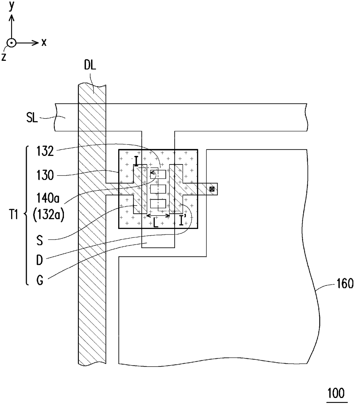
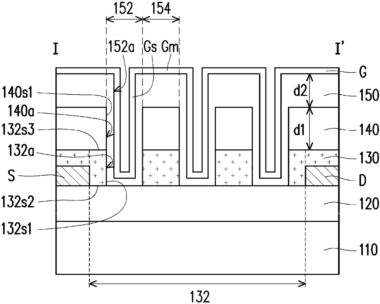
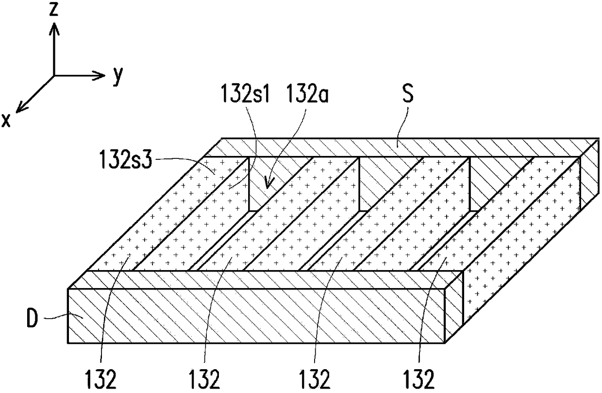
[0059] In the drawings, the thickness of layers, films, panels, regions, etc., are exaggerated for clarity. Throughout the specification, the same reference numerals denote the same elements. It should be understood that when an element such as a layer, film, region, or substrate is referred to as being "on" or "connected" to another element, it can be directly on or connected to the other element, or There may also be intermediate elements. In contrast, when an element is referred to as being "directly on" or "directly connected to" another element, there are no intervening elements. As used herein, "connected" can refer to physical and / or electrical connection. Furthermore, "electrical connection" and "coupling" may mean that there are other elements between the two elements.

[0060] As used herein, "about", "approximately", or "substantially" includes the stated value and the average value within the acceptable deviation range of the specific value determined by a person o...


PUM


Abstract

A pixel structure includes a thin film transistor and a pixel electrode electrically connected to the drain of the thin film transistor. The thin film transistor includes a source, a drain, a semiconductor layer, a first insulating layer, a second insulating layer, and a gate. The semiconductor layer is located on the source and drain and has a channel. The channel is disposed between the source and the drain and has a first via. The first insulating layer is disposed on the semiconductor layer and has a second via that overlaps the first via. The second insulating layer is located on the first insulating layer and in the first via and the second via. The gate is disposed on the second insulating layer.

Description

Technical field [0001] The present invention relates to a semiconductor structure, and in particular to a pixel structure. Background technique [0002] The display panel has the advantages of ultra-thinness, small size and power saving, so it has been widely used in daily life. The display panel includes a pixel array substrate, a counter substrate opposite to the pixel array substrate, and a display medium disposed between the pixel array substrate and the counter substrate. The pixel array substrate includes a substrate, a plurality of thin film transistors arranged on the substrate, a plurality of pixel electrodes electrically connected to the plurality of thin film transistors, a plurality of data lines, and a plurality of scan lines. Among them, the electrical properties of a thin film transistor The pros and cons affect the performance of the display panel most dramatically. [0003] Generally speaking, a thin film transistor includes a source, a drain, a semiconductor lay...

Claims


Application Information

Patent Timeline
IPC IPC(8): H01L27/12H01L29/786
CPCH01L27/1222H01L29/78696
Inventor 刘冠显陈维翰蔡佳宏吴安茹许世华涂峻豪刘竹育
Owner AU OPTRONICS CORP
Features
  • R&D
  • Intellectual Property
  • Life Sciences
  • Materials
  • Tech Scout
  • Unparalleled Data Quality
  • Higher Quality Content
  • 60% Fewer Hallucinations
Learn More