Circuit board structureand manufacture method thereof

A production method and circuit structure technology, applied in multilayer circuit manufacturing, printed circuit manufacturing, printed circuit, etc., can solve problems such as limiting core layer circuit layout and reducing the flexibility of core layer wiring, and achieve the effect of large layout space

Active Publication Date: 2018-06-29
UNIMICRON TECH CORP
View PDF11 Cites 3 Cited by
  • Summary
  • Abstract
  • Description
  • Claims
  • Application Information

AI Technical Summary

Problems solved by technology

However, since the para-copper layer is directly formed on the core layer of the inner line layer, the line layout of the core layer is limited, thereby reducing the wiring flexibility of the core layer

Method used


Image

  • Circuit board structureand manufacture method thereof
  • Circuit board structureand manufacture method thereof
  • Circuit board structureand manufacture method thereof

Examples


Embodiment Construction

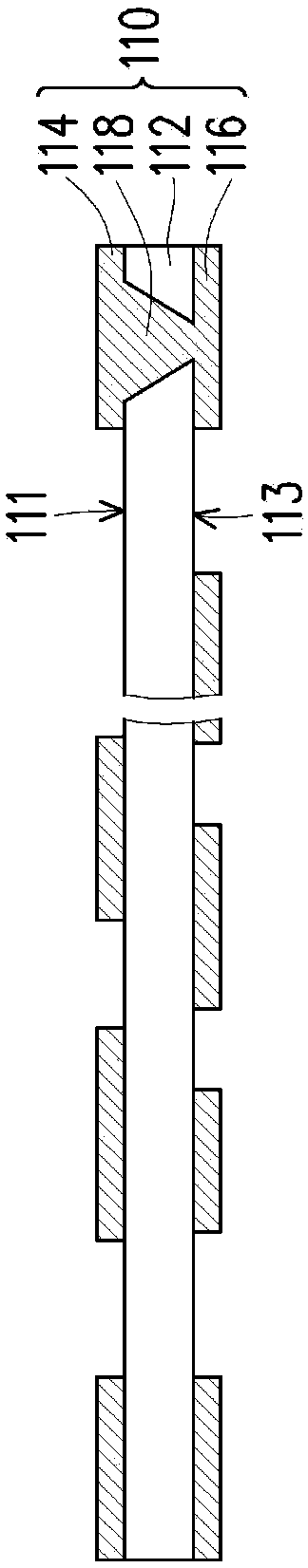
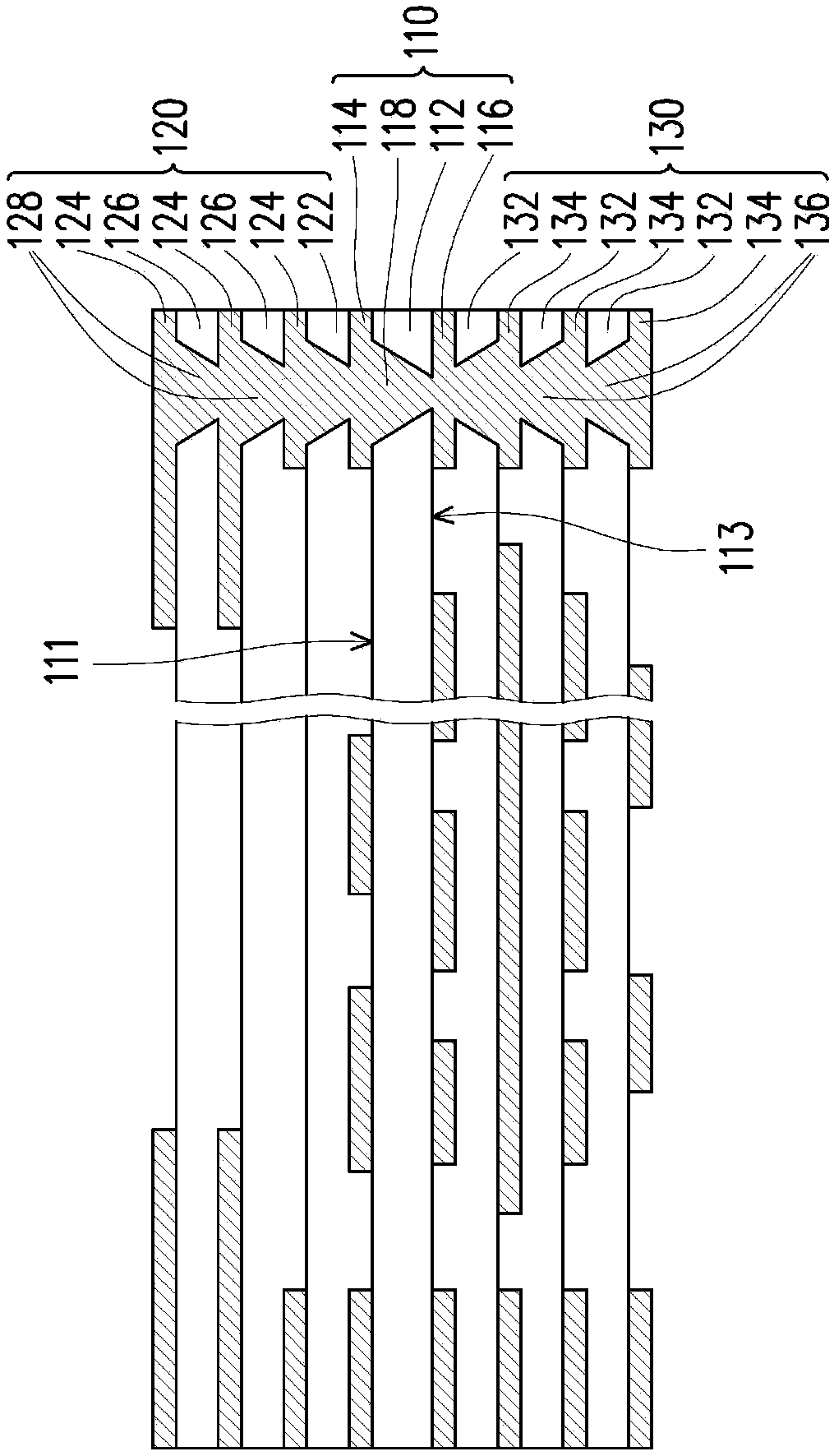
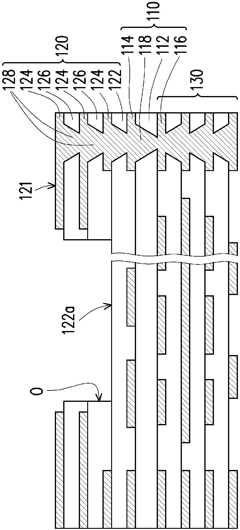
[0068] Figure 1A to Figure 1E Shown is a schematic cross-sectional view of a manufacturing method of a circuit board structure according to an embodiment of the present invention. figure 2 Shown as Figure 1D An enlarged view of the pad area of ​​the circuit board structure. image 3 Shown as Figure 1E The partial top view schematic diagram of the circuit board structure. Regarding the manufacturing method of the circuit board structure of this embodiment, first of all, please refer to Figure 1A , Providing an inner circuit structure 110, wherein the inner circuit structure 110 includes a core layer 112 having an upper surface 111 and a lower surface 113 opposite to each other, a first patterned circuit layer 114 disposed on the upper surface 111, and disposed on the lower surface The second patterned circuit layer 116 on the 113 and the conductive via 118 connecting the first patterned circuit layer 114 and the second patterned circuit layer 116. Here, the material of the fi...


PUM


Abstract

The invention relates to a circuit board structure and manufacture method thereof. The circuit board structure includes an inner layer circuit structure and a first adding layer circuit structure. Theinner layer circuit structure includes a core layer having an upper surface and a lower surface opposite to each other, a first patternized circuit layer arranged on the upper surface, a second patternized circuit layer arranged on the lower surface, and a conducting through hole connecting the first patternized circuit layer and the second patternized circuit layer. The first adding layer circuit structure is arranged on the upper surface of the core layer and covers the first patternized circuit layer. The first adding layer circuit structure at least has a groove. A part of the first patternized circuit layer is exposed from the groove and the outline of a section of the top surface edge of said part is a curved face. The circuit board structure is good in wiring flexibility.

Description

Technical field [0001] The invention relates to a circuit board structure and a manufacturing method thereof, and in particular to a circuit board structure with grooves and a manufacturing method thereof. Background technique [0002] Generally speaking, to make a circuit board structure with grooves, it is usually necessary to make an alignment copper layer on the core layer of the inner circuit structure. The purpose is to follow the process of forming grooves by laser ablating the circuit structure At this time, the alignment copper layer can be regarded as a laser blocking layer to avoid excessive ablation of the circuit structure, and can also be regarded as a laser alignment pattern, which facilitates the laser ablation process. However, since the alignment copper layer is directly formed on the core layer of the inner circuit layer, the circuit layout of the core layer is limited, and the wiring flexibility of the core layer is reduced. Summary of the invention [0003] T...

Claims


Application Information

Patent Timeline
Patent Type & Authority Applications(China)
IPC IPC(8): H05K1/02H05K3/46
CPCH05K1/0298H05K3/4602H05K2201/0338
Inventor 吴明豪刘文芳
Owner UNIMICRON TECH CORP
Why Eureka
Try Eureka