Packaging structure of remote sensor and packaging method thereof
A technology of packaging structure and packaging method, which is applied in the fields of electric solid-state devices, semiconductor devices, semiconductor/solid-state device manufacturing, etc., and can solve the problems of short sensing distance of long-distance sensors and reduced sensing accuracy of chips
- Summary
- Abstract
- Description
- Claims
- Application Information
AI Technical Summary
Problems solved by technology
Method used
Image
Examples
Embodiment Construction
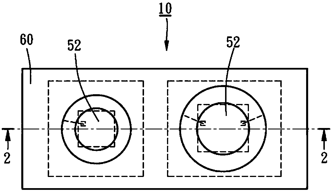
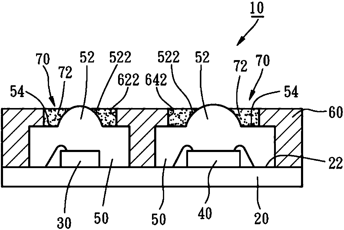
[0035] Please refer to attached image Figure 1~2 The package structure 10 of the remote sensor provided by the first preferred embodiment of the present invention includes a substrate 20, a light-emitting chip 30, a sensing chip 40, two encapsulants 50, a cover 60 and two shielding means 70.
[0036] The substrate 20 has a bearing surface 22, and the substrate 20 can be a printed circuit board (commonly known as PCB), a bismaleimide triazine substrate (commonly known as BT), a glass fiber substrate (commonly known as FR4) or a direct copper clad substrate (commonly known as DBC). ) but not limited thereto, whereby the production cost of the substrate 20 is lower.
[0037] The light-emitting chip 30 is disposed on the carrying surface 22 and electrically connected to the substrate 20 through a wire bonding process. In this preferred embodiment, the light-emitting chip 30 is an LED chip and can be used to emit light.
[0038] The sensing chip 40 is disposed on the carrying su...
PUM
 Abstract
Description
Claims
Application Information


