Device and method for inspecting electronic component
A technology for electronic components and inspection devices, applied in the direction of single semiconductor device testing, etc., can solve problems such as time-consuming inspections
- Summary
- Abstract
- Description
- Claims
- Application Information
AI Technical Summary
Problems solved by technology
Method used
Image
Examples
Embodiment Construction
[0038] Embodiments of the present invention will be described below. In the following description of the drawings, the same or similar components are denoted by the same or similar reference numerals. The drawings are illustrations, and the dimensions and shapes of each part are schematic structures, and should not be interpreted as limiting the technical scope of the invention of the present application as this embodiment.
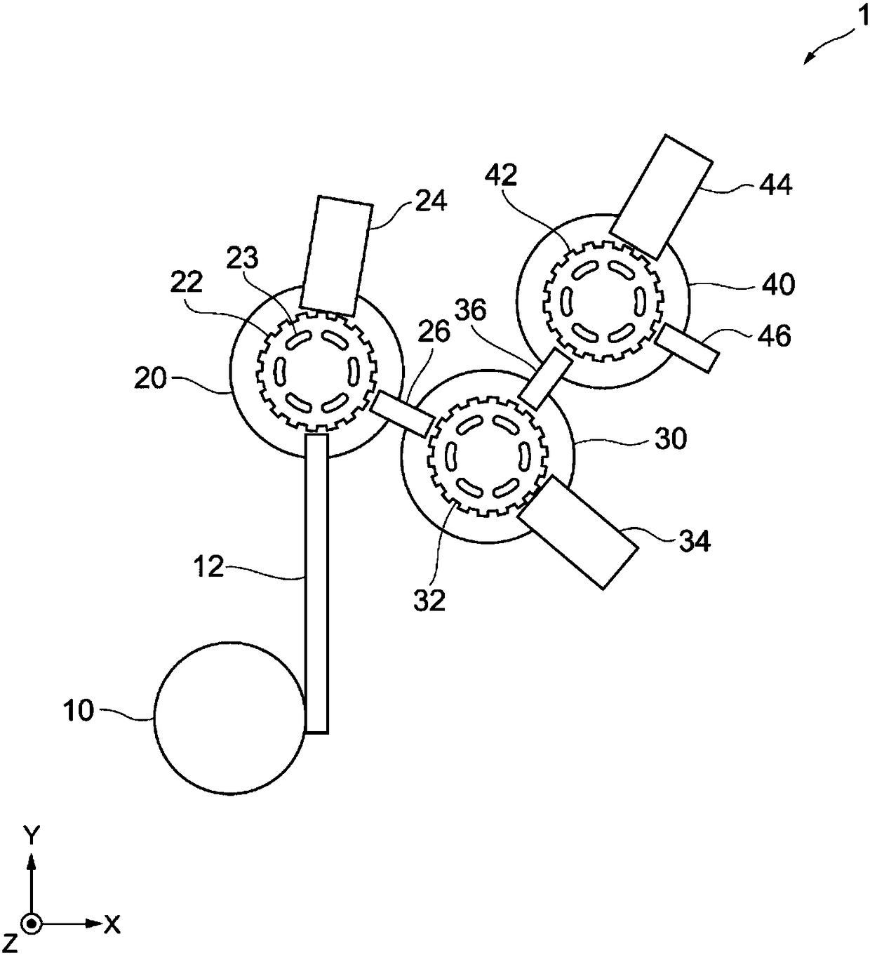
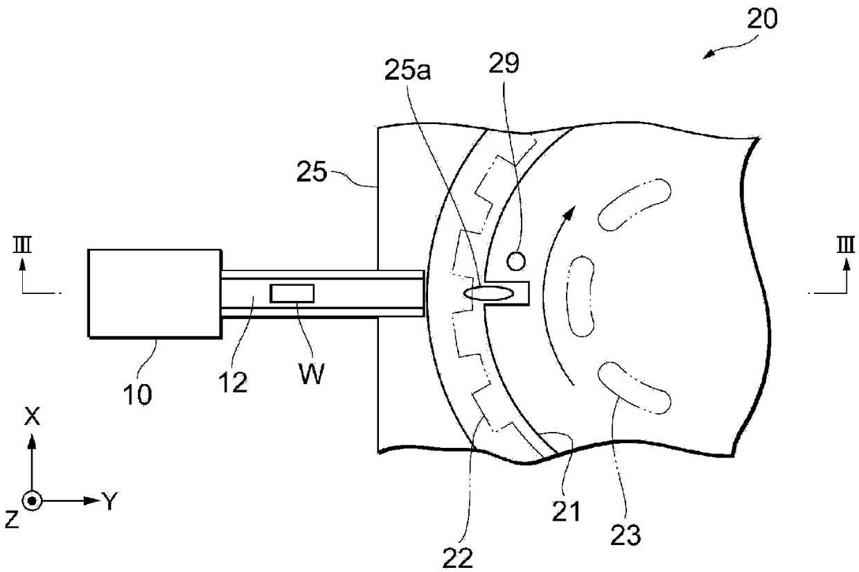
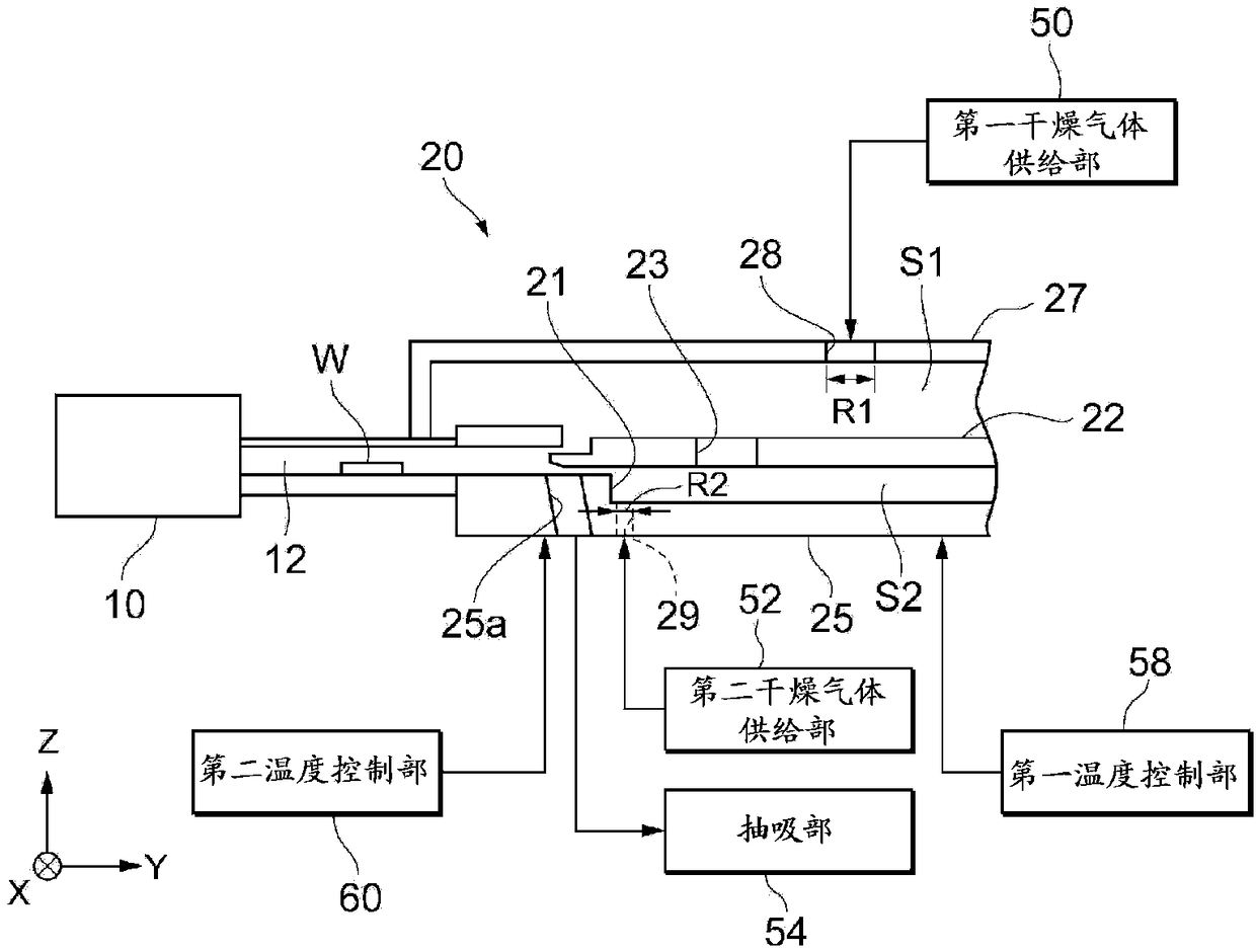
[0039] figure 1 is an overall schematic view of an inspection device according to an embodiment of the present invention, figure 2 and image 3 It is a plan view and a cross-sectional view for explaining the inspection device. Figure 1 to Figure 3 The XYZ axes in the figure are common to each figure, the XY axis direction represents the horizontal direction, and the Z axis direction represents the vertical direction.
[0040] Below, refer to Figure 1 to Figure 4 , an inspection device for an electronic component according to one embodiment of the ...
PUM
 Abstract
Description
Claims
Application Information


