
Flash memory data management method and device and microcontroller

A data management device and data management technology are applied in the direction of electrical digital data processing, input/output process of data processing, error detection of redundant data in operation, etc. problems such as poor capability, to achieve the effect of improving recovery efficiency, improving reliability, and simplifying the recovery process

Active Publication Date: 2018-07-20
ZTE CORP
View PDF5 Cites 5 Cited by
  • Summary
  • Abstract
  • Description
  • Claims
  • Application Information

AI Technical Summary

Problems solved by technology

[0004] The embodiment of the present invention provides a flash memory data management method, device, and microcontroller. The main technical problem to be solved is: the data abnormality of the flash memory in the existing MCU can only be restored by using external data, and the restoration process is cumbersome and inefficient. The problem of poor adaptability

Method used


Image

  • Flash memory data management method and device and microcontroller
  • Flash memory data management method and device and microcontroller
  • Flash memory data management method and device and microcontroller

Examples


Embodiment 1

[0027] In this embodiment, a boot area (BOOT) for storing boot data and an application area (Application, APP) for storing application data are set in the flash memory (Flash Memory), and the data in the boot area and the operation area are respectively backed up in the flash memory. Stored backup boot area (backup BOOT) and backup running area (backup APP), see figure 1 shown.

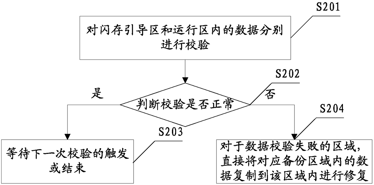
[0028] Based on the above settings, this embodiment can verify and modify the data in the flash memory. For details, see figure 2 shown, including:

[0029] S201: Verifying the data in the boot area and the running area of ​​the flash memory respectively;

[0030] S202: Determine whether the verification is normal, if yes, go to S203; otherwise, go to S204;

[0031] S203: Wait for the trigger or end of the next verification.

[0032] S204: For the area where the data verification fails, directly copy the data in the corresponding backup area to the area for repair, and this step includes:

[003...

Embodiment 2

[0062] This embodiment provides a microcontroller, see Image 6 As shown, a flash memory data management device 1 is included. Wherein the flash memory data management device 1 refers to Figure 7 shown, including:

[0063] The verification module 71 is configured to verify the boot data stored in the boot area of ​​the flash memory and the application data stored in the running area.

[0064] In the present embodiment, a boot area (BOOT) for storing boot data and an application area (Application, APP) for storing application data are set in the flash memory (Flash Memory), and the data in the boot area and the operation area are respectively set in the flash memory. Backup boot area (backup BOOT) and backup operation area (backup APP) for backup storage.

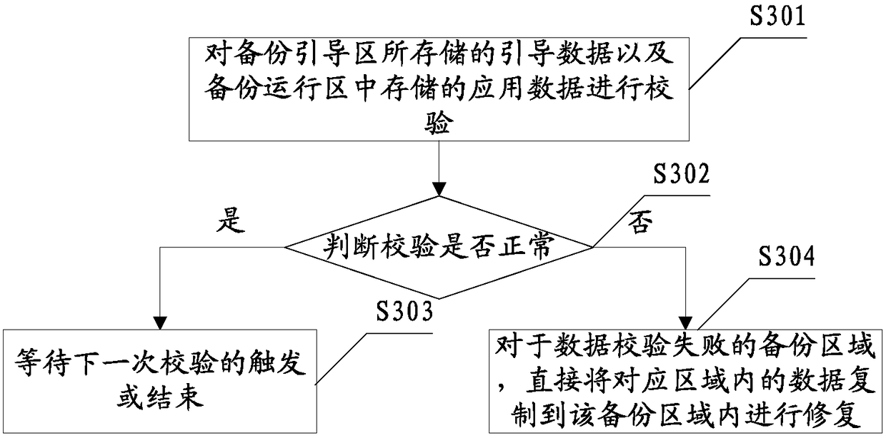
[0065] The repair processing module 72 is used to copy the boot data in the backup boot area to the boot area for repair when the boot data verification in the boot area fails; and when the application data verification ...


PUM


Abstract

The invention provides a flash memory data management method and device and a microcontroller. The method comprises the following steps of: setting a guiding area for storing guiding data and an operation area for storing application data in a flash memory, and setting a backup guiding area and a backup operation, which are respectively used for carrying out backup storage on data in the guiding area and the operation area, in the flash memory; respectively verifying the data in the guiding area and the operation area of the flash memory; and when the verification of the data in a certain areafails, directly copying the data in the corresponding backup area into the area to carry out recovery. According to the method, data in MCU flash memories can be verified through a verification mechanism, and when the verification fails to cause exceptions, rapid modification is directly carried out through backup data in the flash memories, so that the recovery process can be simplified, the recovery efficiency can be enhanced, the self-adaptive ability of the flash memories can be enhanced, the reliability of the MCUs can be enhanced, and particularly, the reliability, in power supply applications, of the MCUs can be enhanced.

Description

technical field [0001] The invention relates to the communication field, in particular to a flash memory data management method, device and microcontroller. Background technique [0002] Microcontrollers (Microcontroller Unit, MCU, also known as single-chip microcomputers) are increasingly widely used in the field of communication. For example, with the rapid development of switching power supplies in the direction of digitalization and intelligence, the design is becoming more and more complex, and reliability is also being challenged. Therefore, the current switching power supply more and more uses the MCU to realize the core function, so the operation stability of the MCU is directly related to the product quality of the power supply. [0003] The MCU fetches instructions directly by running on its internal on-chip flash memory (Flash Memory). Due to its own characteristics, flash memory has a limited number of times of erasing and writing, and there is a certain probab...

Claims


Application Information

Patent Timeline
Patent Type & Authority Applications(China)
IPC IPC(8): G06F3/06G06F11/14
CPCG06F3/0614G06F3/0638G06F3/0679G06F11/1402Y02D10/00
Inventor 熊毅张正清
Owner ZTE CORP
Learn More