Back-illuminated image sensor and manufacturing method thereof and electronic device
A technology of an image sensor and a manufacturing method, applied in the directions of radiation control devices, circuits, electrical components, etc.
- Summary
- Abstract
- Description
- Claims
- Application Information
AI Technical Summary
Problems solved by technology
Method used
Image

Examples
Embodiment 1
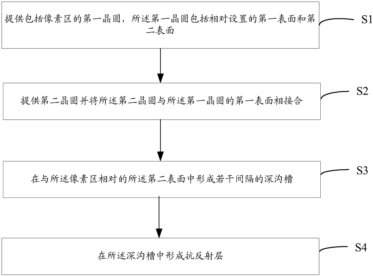
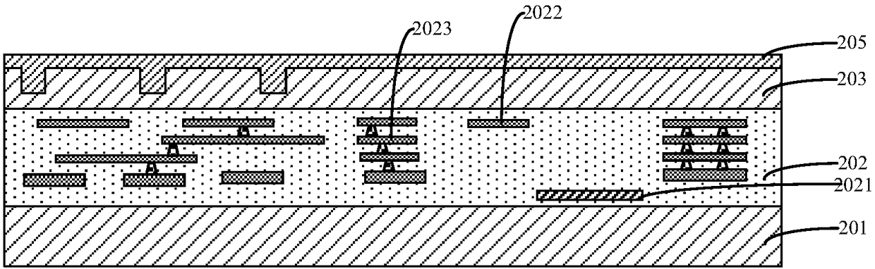
[0075] Below, refer to figure 1 as well as Figure 2A to Figure 2F The detailed steps of an exemplary method of the manufacturing method of the back-illuminated image sensor proposed by the embodiment of the present invention will be described. in, figure 1 It is a schematic flowchart of a manufacturing method of a back-illuminated image sensor according to an embodiment of the present invention, 2A to 2A Figure 2F It is a cross-sectional view of a structure formed in related steps of a manufacturing method of a back-illuminated image sensor according to an embodiment of the present invention.
[0076] Such as figure 1 As shown, the manufacturing method specifically includes the following steps:
[0077] Step S1: providing a first wafer including a pixel region, the first wafer including a first surface and a second surface oppositely arranged;
[0078] Step S2: providing a second wafer and bonding the second wafer to the first surface of the first wafer;
[0079] Step ...
Embodiment 2
[0169] An embodiment of the present invention provides a back-illuminated image sensor, which is prepared by the manufacturing method in the first embodiment above. The back-illuminated image sensor may be an integrated circuit including a radio frequency (RF) device or an intermediate product of an integrated circuit.
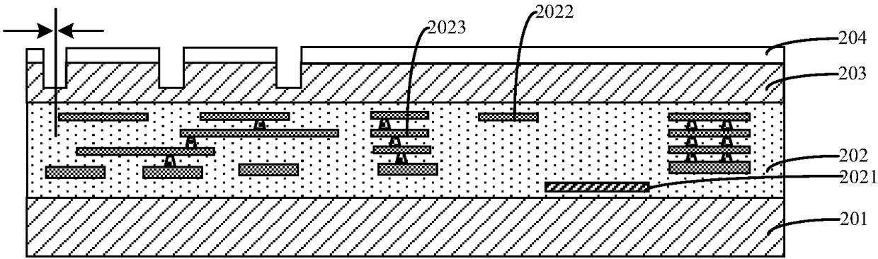
[0170] Below, refer to Figure 2F A structure of a back-illuminated image sensor proposed by an embodiment of the present invention will be described. in, Figure 2F It is a cross-sectional view of the structure of the back-illuminated image sensor of the embodiment of the present invention.
[0171] Such as Figure 2F As shown, the back-illuminated image sensor of this embodiment includes:
[0172] a first wafer comprising a pixel region, the first wafer comprising a first surface and a second surface oppositely disposed;
[0173] A second wafer 203, the second wafer is bonded to the first surface of the first wafer;
[0174] a deep trench located on th...
Embodiment 3
[0209] An embodiment of the present invention provides an electronic device, which includes an electronic component and a back-illuminated image sensor electrically connected to the electronic component. Wherein, the back-illuminated image sensor includes the back-illuminated image sensor manufactured according to the manufacturing method of the back-illuminated image sensor described in the first embodiment, or includes the back-illuminated image sensor described in the second embodiment.
[0210] The electronic device can be any electronic product or equipment such as mobile phone, tablet computer, notebook computer, netbook, game console, TV, VCD, DVD, navigator, camera, video camera, recording pen, MP3, MP4, PSP, etc. It is an intermediate product with the above-mentioned back-illuminated image sensor, such as a mobile phone motherboard with this integrated circuit, etc.
[0211] in, image 3 An example of a mobile phone handset is shown. The mobile phone handset 300 is ...
PUM
 Abstract
Description
Claims
Application Information
 - R&D Engineer
- R&D Manager
- IP Professional
- Industry Leading Data Capabilities
- Powerful AI technology
- Patent DNA Extraction
Browse by: Latest US Patents, China's latest patents, Technical Efficacy Thesaurus, Application Domain, Technology Topic.
© 2024 PatSnap. All rights reserved.Legal|Privacy policy|Modern Slavery Act Transparency Statement|Sitemap