High frequency ultrasound transducer and method for manufacture
A transducer, ultrasonic technology, applied in the direction of fluid using vibration, ultrasonic/sonic/infrasonic diagnosis, application, etc., can solve problems such as error-prone, time-consuming, etc.
Active Publication Date: 2018-07-31
FUJIFILM SONOSITE
12 Cites 0 Cited by
AI-Extracted Technical Summary
Problems solved by technology
At these small sizes, the challenge of aligning and bonding the individual ...
Method used
[0024] FIGS. 1A-1D and the following description provide a brief overview of the various steps that need to be performed in fabricating a high frequency ultrasonic transducer in accordance with aspects of the disclosed technology. Additional details on some aspects of the manufacturing method can be found in U.S. Patent Publication Nos. US2013/0207519, US2013/0140955, US2014/0350407, and US2015/0173625, all of which are assigned to Fujifilm SonoSite Corporation, the assignee of the present application, and are incorporated herein by reference method is incorporated into this article as a whole. In one embodiment, a rectangular sheet of piezoelectric material 50 is mounted on a planar fabrication disk with the lower surface facing up, and then processed using a patterning tool such as an excimer laser. A laser or other patterning tool is then used to fabricate the array of transducer elements 58 in the sheet of piezoelectric material and to fabricate a plurality of via holes 60 spaced around the perimeter of the transducer array. As shown in Figure IB, the array includes a plurality of transducer elements 58a, 58b, 58c, and so on. In one embodiment, each transducer element 58 is further split along its length at the center of each element to avoid vibrating in unintended modes. In the illustrated embodiment, the kerf slots defining the array elements and further dicing are shown, the length of the kerf slots being less than the width of the piezoelectric material. However, it is also possible to extend the cutout to the edge of the piezoelectric material 50 .
[0034] To improve this assembly technique, the channel or channels connecting each transducer element to the traces should be designed such that each channel forms a raised rib as it extends up the side walls of the frame 70. As shown in Figure 3, a plurality of channels 100a, 100b, 100c, etc., are cut in powder filled epoxy 72 at a pitch equal to that of every other transducer element, eg, all odd numbered transducer elements , while creating staggered channels on the opposite side of the frame, aligned with all even-numbered transducer elements. Or channels could be created only on one side of the frame 70 where each transducer element is aligned. In one embodiment, the depth of the channel aligned with each transducer element decreases as the channel extends outward from the transducer element. About halfway up the side walls of the frame 70, the channel depth decreases a bit at which point the "channel" begins to extend outward from the epoxy surface to form outwardly extending ribs 102a, 102b, 102c, etc.; in one implementation In one example, the ribs 102 are formed by ablating the powder-filled epoxy 72 on either side of the defined rib area. In one embodiment, a laser is used to form a plurality of score lines along the top surface of each rib 102 to increase the surfac...
Abstract
An ultrasound transducer has an array of transducer elements that are electrically coupled to electrical conductors. In one embodiment, the conductors are included in a flex circuit and engage a conductive surface formed on a number of outwardly extending ribs on a frame that holds the ultrasound array. In one embodiment, the flex circuit includes an alignment feature that engages a correspondingregistration feature on the frame so that the traces on the flex circuit align with the ribs on the frame.
Application Domain
Ultrasonic/sonic/infrasonic diagnosticsMechanical vibrations separation +2
Technology Topic
Electrically conductiveEngineering +6
Image
Examples
- Experimental program(1)
Example Embodiment
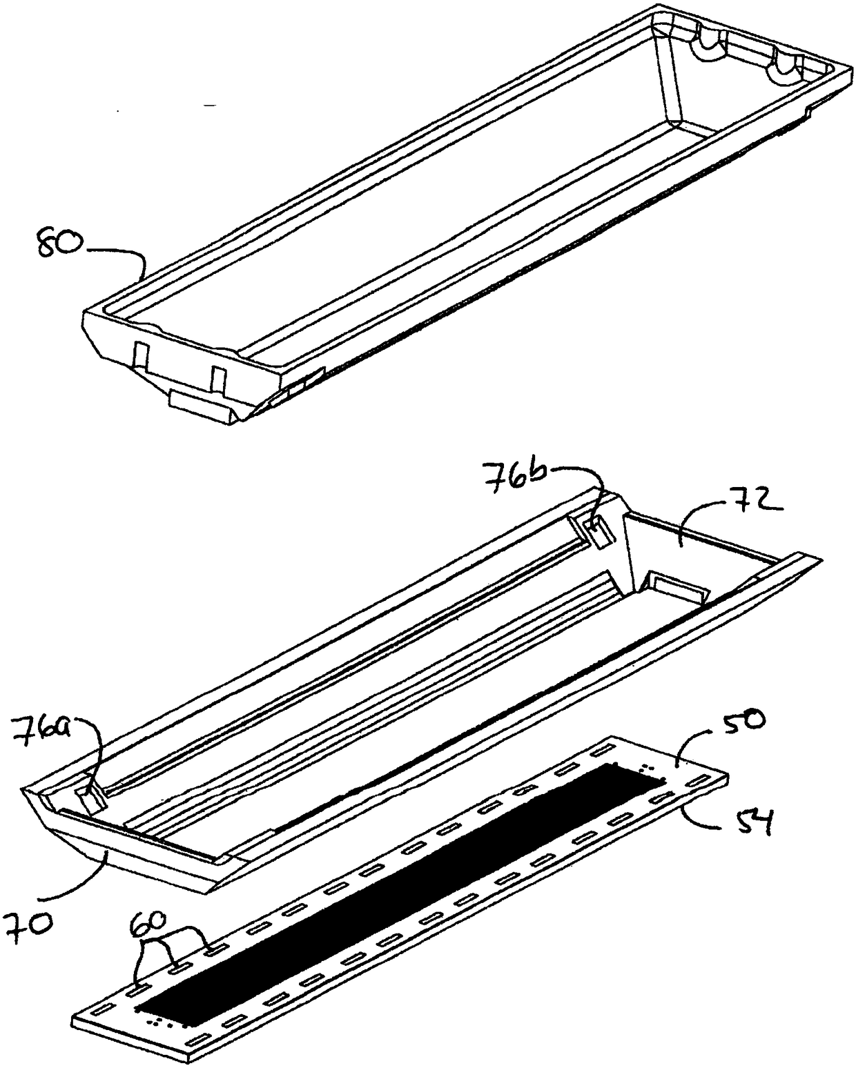
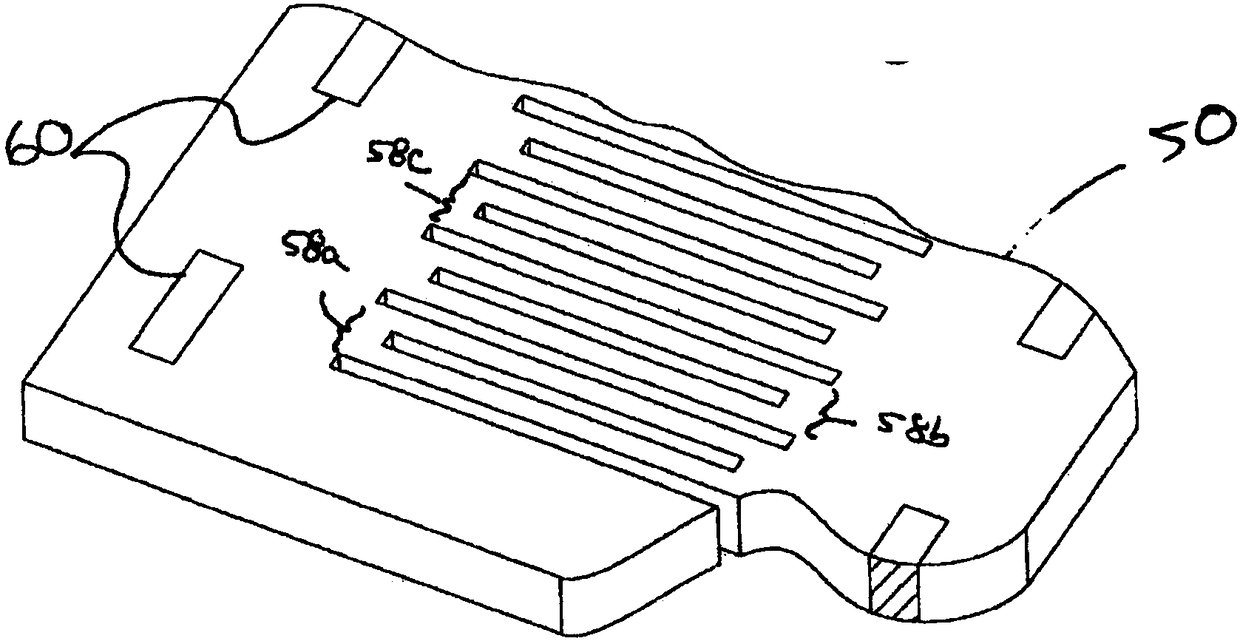
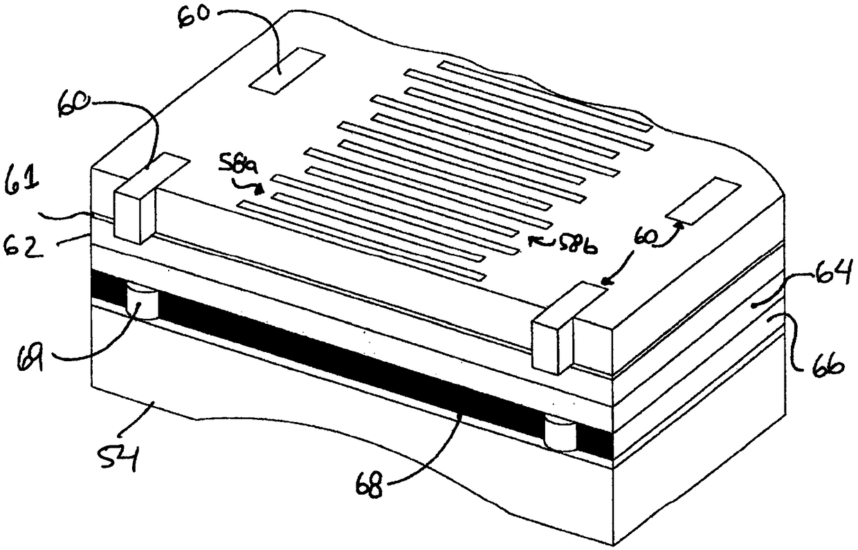
[0023] As mentioned above, one of the challenges associated with manufacturing high frequency ultrasound transducers is performing the step of electrically connecting multiple conductive leads or traces to the individual transducer elements of the transducer array without interrupting the array transduction. performance of device components. Previously the conductive traces had to be manually aligned to the transducer elements, after which they were handled with care until the manufacturing process was complete. Accidental bumping of the transducer assembly or improper alignment of the traces can result in part rejection. This problem becomes more acute as the operating frequency of ultrasonic transducers increases and the transducer elements are miniaturized. The techniques described herein simplify the manufacturing process steps of aligning and connecting the conductive traces to the individual transducer elements of a transducer array.
[0024] Figures 1A-1D and the following description give a brief overview of the many steps to be performed in the manufacture of high frequency ultrasonic transducers in accordance with aspects of the disclosed technology. Additional details on some aspects of the manufacturing method can be found in U.S. Patent Publication Nos. US2013/0207519, US2013/0140955, US2014/0350407, and US2015/0173625, all of which are assigned to Fujifilm SonoSite Corporation, the assignee of the present application, and are incorporated herein by reference method is incorporated into this article as a whole. In one embodiment, a rectangular sheet of piezoelectric material 50 is mounted on a planar fabrication disk with the lower surface facing up, and then processed using a patterning tool such as an excimer laser. A laser or other patterning tool is then used to fabricate the array of transducer elements 58 in the sheet of piezoelectric material and to fabricate a plurality of via holes 60 spaced around the perimeter of the transducer array. like Figure 1B As shown, the array includes a plurality of transducer elements 58a, 58b, 58c, and so on. In one embodiment, each transducer element 58 is further split along its length at the center of each element to avoid vibrating in unintended modes. In the illustrated embodiment, the kerf slots defining the array elements and further dicing are shown, the length of the kerf slots being less than the width of the piezoelectric material. However, it is also possible to extend the cutout to the edge of the piezoelectric material 50 .
[0025] The gaps between the transducer elements and in the further cut-out slots should be filled with a suitable acoustically soft material, such as soft epoxy using vacuum pressure impregnation techniques. After the cutouts are filled, the surfaces are lapped or ground to just the right level for the piezoelectric material and then coated with a conductive metal of gold or chromium plus gold to form a ground conductor on the lower surface of the sensor. The via hole 60 is covered with conductive epoxy and filled with plating through the hole. Now that the vias are plated and filled, the vias 60 can form a conductive path to the conductors on the front of the transducer array. During operation, conductors on the front surface of the transducer are typically connected to electrical ground, while drive signals are applied to the top of selected transducer elements through conductive leads (not shown). When excited by a signal, the transducer element vibrates to produce an acoustic ultrasound signal. During a receive cycle, acoustic energy strikes the transducer element and produces a signal on the leads that is read by signal processing circuitry (not shown).
[0026] like Figure 1C and 1D As shown, the front surface of the transducer is connected to lens material 54 by a plurality of matching layers. In one embodiment, two powder-filled epoxy matching layers 62 and 64 are applied to the conductor-coated surface 61 of the piezoelectric material 50, each forming part of a four-layer matching layer system. The matching layers 62 and 64 are each overlapped after application to ensure that the layers have the proper thickness.
[0027] Lens material 54 is later bonded to the outer surface of matching layer 64 . In one embodiment, the lens material 54 is made of Rexolite TM Polymers such as polystyrene. However, other lens materials may be used. In one embodiment, the lens 54 is coated with an adhesive layer, such as cyanoacrylate (CA) glue 68 that adheres to a particular lens material. The CA glue 68 can be bonded to the lens surface and can be adhered to the lens surface by other adhesives more commonly used to make acoustic matching layers. The layer of cyanoacrylate glue 68 is ground to a thickness suitable for use as an acoustic matching layer at the array frequency, eg a quarter wave matching layer. In one embodiment, CA cemented cover lens 54 is bonded to matching layer 64 with powder filled epoxy adhesive 66 . Adhesive 66 forms the three-quarter wavelength matching layer of the four-layer system, and CA layer 68 forms the fourth of the four layers. Prior to adhering lens 54 to matching layer 64 , a series of cuts 67 are made in matching layers 62 and 64 . like Figure 1D As shown, cutout 67 is aligned with the space between transducer elements 58 .
[0028] The thickness of adhesive 66 required to fabricate the third matching layer is controlled by placing a plurality of spacer elements 69 around the lower perimeter of the sheet of piezoelectric material 50 . The spacer elements 69 are overlapped to a desired thickness to form columns of a selected height such that the adhesive 66 forms a quarter wavelength matching layer. With the spacer element 69 in place, adhesive 66 is placed over the matching layer that has been applied to the piezoelectric sheet surface, and the CA-coated lens material 54 is pressed against the spacer 169 so that the desired The distance (from the surface of the uppermost matching layer that has been applied to the plated piezoelectric material 50 in advance) cements the lens. Adhesive 66 applied under vacuum fills cutout grooves 67 formed in first and second matching layers 62 , 64 . In one embodiment, the components of the matching layers 62, 64, 66 are described in commonly assigned US Pat. Nos. 7,750,536 and 8,343,289, which are hereby incorporated by reference in their entirety.
[0029] A sheet of piezoelectric material 50, acoustic matching layer, and lens material 54 (lens side down) are then mounted to the fabrication disc and overlapped so that the transducer element has the desired thickness.
[0030]A conductive metal frame 70 made of metal such as molybdenum is bonded to the upper surface of the transducer array with conductive epoxy. Thus, the conductive frame is electrically connected to the conductive material of the front surface of the transducer array through the conductive paths made by the filled vias 60 . The frame 70 has an open bottom surface so that the upper surface of the transducer element is accessible through the opening in the bottom of said frame 70 . The frame 70 has sloped sidewalls to collectively form a slot on the transducer array 58 . In the illustrated embodiment, the frame is conductive to create an electrical path through the vias from the conductive surface on the distal side of the transducer. However, it is also possible to utilize a non-conductive frame and use separate conductors such as metal foil, wire or other conductors to electrically connect the conductive surface on the distal side of the transducer to the ground/shield layer containing the signal trace flex circuit.
[0031] After the frame 70 is bonded to the transducer array, a cover is placed over the transducer elements and a powder filled epoxy 72 material is added to the open side of the frame 70 . In one embodiment, the powder added to the bonding material is powdered silica, which can add texture to the surface of the epoxy resin after laser processing. The release agent coated mold 80 is then pressed into the epoxy 72 as it cures to form a plurality of desired feature shapes in the frame. In one embodiment, the shape may include a pair of recesses 76a, 76b on the side walls of the frame at locations outside the length of the ultrasonic array. Additional recesses may be formed on opposing side walls of the frame (not shown).
[0032] figure 2 A close-up view of one corner of the frame 70 and recess 76b formed in the epoxy 72 is shown. Registration features 78 are disposed in each recess 76 and are used to align the electrical traces of the flex circuit with the transducer elements, as will be described below. In one embodiment, registration features 78 are preferably made of powder filled molded epoxy material and are precisely laser machined to specific tolerances, eg, +/- 5 microns. The registration feature 78 may be secured within the recess 76 using an adhesive. In some embodiments, the undersized recesses 76 may be molded into epoxy and sized with a laser or other micromachining tool so that the recesses are precisely positioned at the rib locations (described below). After the recesses have been precisely positioned and adjusted, registration features 78 are glued into the recesses so that corresponding alignment features can be mounted on the flex circuit. In some other embodiments, a blob of excess epoxy or other glue can be placed on the frame and micromachined with a laser or the like into the registration features. Registration features on the frame and corresponding alignment features on the flex circuit align the exposed traces of the flex circuit with the conductive ribs on the frame.
[0033] The powder-filled epoxy in the transducer frame 70 is then machined using an excimer laser to create channels that connect to the individual transducer elements of the transducer array. As discussed in the aforementioned patent application, a laser is used to create a pattern of channels extending from the top surface of each transducer element and a portion of the sidewall of the transducer frame. Historically, the flex circuit has been secured to the frame before powder-filled epoxy is added to the frame so that the exposed circuit traces are covered with epoxy. A patterning tool such as an excimer laser is then used to dig through the epoxy, thereby exposing a portion of the circuit traces on the flex. While this works well, it requires manual alignment of the traces on the flex circuit with the transducer elements before securing to the frame. Additionally, until the transducer is encapsulated in the material used to bring the flex circuit and transducer assembly together, the assembly is fragile.
[0034] To improve this assembly technique, the channel or channels connecting the transducer elements to the traces should be designed such that each channel forms a raised rib as it extends up the side walls of the frame 70 . like image 3 As shown, a plurality of channels 100a, 100b, 100c, etc., are cut in powder-filled epoxy 72 at a pitch equal to that of every other transducer element, such as all odd-numbered transducer elements, while at The other side of the frame creates staggered channels that align with all even-numbered transducer elements. Or channels could be created only on one side of the frame 70 where each transducer element is aligned. In one embodiment, the depth of the channel aligned with each transducer element decreases as the channel extends outward from the transducer element. About halfway up the side walls of the frame 70, the channel depth decreases a bit at which point the "channel" begins to extend outward from the epoxy surface to form outwardly extending ribs 102a, 102b, 102c, etc.; In one example, the ribs 102 are formed by ablating the powder-filled epoxy 72 on either side of the defined rib area. In one embodiment, a laser is used to form a plurality of score lines along the top surface of each rib 102 to increase the surface area of the top of the rib 102 and ensure the robustness of the gold electrode during the pressing process of A flexible circuit is secured to a portion of the surface of the raised rib.
[0035] After the channels and ribs are patterned in epoxy, the top surface of the transducer assembly is plated and machined such that the channels 100 and the tops of the ribs 102 are plated with a conductive layer. In one embodiment, the conductive material is applied by sputter coating a metal layer of gold or gold plus chromium on the surface of the transducer array including the top surface, transducer elements and ribs. A resist layer is then applied over the transducer and exposed in the areas where the conductive material will be removed using photolithographic techniques. In one embodiment, conductive material is removed between the transducer elements, between the conductive path channel areas, and should be removed from all sides of the ribs. Use a chemical etch material to remove conductive material where it is not needed. Finally, a laser is used to remove any traces of conductive material left after the etching process.
[0036] Following the laser etch laser (LEL) process, a conductive path exists between the top surface of each transducer element and the corresponding rib 102 on the frame 70 . A flexible circuit having a plurality of exposed traces is then secured to the frame such that the exposed traces are aligned and engaged with corresponding ribs on the frame to create an electrical connection between the traces and the transducer elements. One of the advantages of this method is that there is no need to fix the flex circuit to the transducer assembly, while the top surface of the transducer is coated with a conductive material. Therefore, the flex circuit connections are less likely to be damaged during handling of the transducer. Additionally, more transducer assemblies can be installed into the sputter chamber because the flex circuit is not attached when the coating is applied. Thus, more transducer assemblies can be processed at one time.
[0037] image 3 In the illustrated embodiment, each rib 102 terminates at the same height on the transducer's frame wall. In another embodiment, the ribs 102 may terminate at different heights on the walls of the frame so that staggered traces connect to the ribs. For example, the traces on two or more flex circuits may be staggered or interleaved if the connections to the transducer elements are to be smaller than the distance between traces on a single flex circuit. For example, one set of traces 1, 3, 5, etc. could be placed in one layer of a flex circuit, and traces 2, 4, 6, etc. could be placed in a different layer of a flex circuit that could be The exposed traces are withdrawn. Exposed portions of the traces in each layer may be bonded to ribs that extend to different heights on the transducer frame wall. A similar technique for interleaving traces is disclosed in the above-referenced Published US Patent Application Publication No. US2013-0140955A1, which is hereby incorporated by reference in its entirety.
[0038] Figure 9 An example of an ultrasonic transducer with two sets of ribs at different levels is shown. In the example shown, the frame includes a first set of ribs 250 at a first height on the side walls of the frame, and a second set of ribs 252 extending upwardly on the frame. The ribs on each layer are staggered. One flex circuit (not shown) with exposed traces engages the rib 252 , while the other flex circuit with exposed traces engages the rib 250 . It should be understood that more than two layers of ribs may be formed in the epoxy material if desired.
[0039] In one embodiment, the exposed traces on the flex circuit are bonded to the ribs 102 with a non-conductive adhesive. Because the surface of the filled epoxy matrix is rough (on a microscopic scale) after laser machining, the matrix-fill material-coated particles on top of the ribs can be used to pass through when the flex circuit and ribs are bonded together. Adhesive and conductive nails that engage flex circuit conductors. One or more grounds of the flex circuit are connected to the metal frame 70 of the transducer assembly with conductive epoxy.
[0040] While flex circuit manufacturers can form traces with the high precision pitch they desire, they often cannot control the distance between the edge of the flex circuit and the start of the trace with the same tolerance. The distance between the edge of the flex circuit and the start of the trace can vary widely. Therefore, one cannot simply align the edge of the flex circuit with features on the transducer frame while expecting that the traces can be aligned with the conductors connected to the transducer elements. Figure 4 Is a schematic diagram of a typical flex circuit 150 including a plurality of conductive exposed traces 152a, 152b, 152c, . . . 152h. Usually the distance between traces 152 is very precise. However, the distance between edge 154 and the closest trace 152a or between edge 156 and the closest trace 152h can vary significantly between different flex circuits. To solve this problem, use the figure 2 The registration feature 78 is shown.
[0041] like Figure 5 As shown, one embodiment of the disclosed technology provides alignment holes or alignment features 160a, 160b in the flex circuit. Such features may be formed using a laser at a predetermined distance 166, 168 from a reference point (eg, the closest trace). It should be appreciated that the alignment holes 160 can be mounted over corresponding registration features 78 placed on the frame 70 so that when the registration features 78 are placed in the alignment holes 160, the traces on the flex circuit The wires can be aligned with corresponding ribs on the frame.
[0042] According to another aspect of the disclosed technology, some embodiments of the flex circuit 150 include holes or vias 170 cut between the electrical traces 152 . In one embodiment, the holes 170 are located between traces on the flex circuit. In another embodiment, the holes 170 are located between flex circuit traces at different intervals (or varying intervals). The holes 170 allow the adhesive used to secure the flex circuit to the rib 102 to squeeze out and form a rivet-shaped cap that facilitates securing the flex circuit to the transducer frame. Image 6 is a schematic illustration of an example of a flexible circuit 150 secured to a plurality of ribs 102 on the frame 70 . A portion of the adhesive used to secure the flex circuit to the rib on the frame is pressed through the hole 170 to form a rivet 176 that facilitates maintaining contact between the rib and the trace and prevents the flex circuit from detaching from the frame 70. break away.
[0043] Figure 10 Another example is shown of how a flex circuit 260 having exposed traces (now shown) on its underside is secured to the plurality of conductive ribs 102 to electrically connect the traces in the flex circuit to the transducer elements. The conductive rib faces upward and engages the exposed trace facing downward. The flex circuit 260 is secured to the frame with an adhesive as described above.
[0044] In some embodiments, it may not be possible or desirable to place all of the traces that connect to the elements of the transducer array on a single flex circuit. One such example is a medical device such as a prostate probe comprising a linear array of 512 transducer elements. In one embodiment, in order to reduce the size of the sleeve that carries the traces to the transducer elements, the traces are divided into four flex circuits stacked on top of each other. For example, one flex circuit has traces for even-numbered components between part numbers 0-127, another has traces for even-numbered components between part numbers 128-255, and another has traces for even-numbered components between part numbers 256- 383 and another trace for even numbered components between part numbers 384-512. Another stack of four flex circuits was used to connect to the odd numbered transducer elements on the other side of the array. Two stacks of four flexible circuits are then arranged at the location of the sleeve (not shown) extending from the distal end of the probe at which the transducer is located to the connector at the proximal end of the probe.
[0045] Figure 7One method of securing multiple flex circuits to a transducer array is shown such that the traces on the flex circuits align with the ribs on the transducer frame. In the example shown, a plurality of flex circuits 212a, 212b, 212c, and 212d are placed in a jig 200 that includes a plurality of tabs 210a, 210b...2101 formed therein. In one embodiment, the flex circuit is secured to a carrier bar 220 placed below the flex circuit. In one embodiment, the carrier bar 220 has at least one (and preferably two) alignment holes 222a, 222b sized to fit over corresponding registration features on the ultrasound frame. The sides of the flex circuit are trimmed so that adjacent traces on adjacent flex circuits will maintain the same spacing, and holes or alignment features are created in the laser in the flex circuit 212 so that they fit together when placed in the jig. over the tab 210, and the traces will line up precisely. When the holes on the flex circuit are placed over the tabs 210 in the jig 200 , the traces on the flex circuit are positioned at known locations relative to the holes 222 a , 222 b on the carrier bar 220 . Once the flex circuit 212 is positioned on the tab 210 and secured to the carrier bar 220, excess flex circuit material in the area of the tab 210 can be removed (e.g., with a laser), and the carrier bar 220 can be placed on the ultrasonic transducer. on the frame of the device such that the alignment holes 222a, 222b fit over the registration features 78 on the frame. In the illustrated embodiment, the lengths of flex circuit extending from the transducer array are stacked such that the traces in the flex circuit overlap vertically after exiting the array support. However, if limiting the size of the connection to the transducer is not an important design issue, the flex circuit could also extend side-by-side to the connector.
[0046] Figure 8 A portion of a transducer 240 that may be used with a prostate probe or other medical device is shown. In one embodiment, the transducer has 512 (or more) transducer elements. To keep the probe as narrow as possible, the flex circuit 242 is angled so that the trace is in line with the transducer elements in the transducer array area, then turned 77 degrees (but can be operated at any angle), and then aligned with the transducer run in the direction aligned with the length of the array. Additional flex circuits (not shown) are secured to the frame to carry signals from other transducer elements. Lengths of flex circuits are stacked vertically rather than side-by-side because they run the length of the probe, allowing the probe diameter to be smaller.
[0047] Figure 11 An example of a transducer assembly is shown that includes a plurality of flexible circuits with traces electrically connecting individual transducer elements in the array. In the example shown, the transducer elements are electrically connected to traces in the flex circuits 212a, 212b, 212c, and 212d positioned side-by-side along the array length direction 270 . The alignment of the traces in the flex circuit is referenced by the location of the alignment holes 222a, 222b cut into the carrier bars. The traces in the flex circuit are aligned with corresponding ribs on the transducer frame by placing the holes 222 in the carrier rod over the registration features 78a, 78b on the transducer frame. In the illustrated embodiment, the flex circuits are positioned side-by-side for connection to the transducer elements, but are arranged to be stacked on top of each other and extend in a direction 270 generally in the direction of the long axis of the transducer array. This makes the connection to the transducer much narrower than if the flex circuit were placed side-by-side. For internal imaging probes, the reduced width of the flex circuit increases patient comfort. In the example shown, flex circuits 212, 212b, 212c, 212d carry signals to even (or odd) numbered transducer elements, and a matched set of stacked flex circuits on the other side of the transducer array Circuitry (not shown) is used to transmit signals to odd (or even) sensor elements. In one embodiment, eight flex circuits, each with 64 traces, are used to route signals to and from the 512-element transducer array. In one embodiment, a 512 element side-firing high frequency transducer array is useful in a prostate imaging probe.
[0048] As noted above, it should be appreciated that for the purpose of illustrating the invention, specific embodiments of the technology disclosed herein have been described, but various modifications may be made without departing from the scope of the invention. For example, there is no need to mount the transducer frame and registration features on the flex circuit as posts and holes together. Other shapes, such as key and keyway, may be used. Alternatively posts or other shapes may be fixed in known locations on the flex circuit and holes or other shapes may be formed in the frame so that the flex circuit aligns with the ribs on the frame. Accordingly, the invention is not to be restricted except in accordance with the appended claims.
PUM


Description & Claims & Application Information
We can also present the details of the Description, Claims and Application information to help users get a comprehensive understanding of the technical details of the patent, such as background art, summary of invention, brief description of drawings, description of embodiments, and other original content. On the other hand, users can also determine the specific scope of protection of the technology through the list of claims; as well as understand the changes in the life cycle of the technology with the presentation of the patent timeline. Login to view more.