High-speed superjunction lateral insulated gate bipolar translator

A technology of bipolar transistors and insulated gates, applied in semiconductor devices, electrical components, circuits, etc., can solve the problems of high cost, high power consumption at shutdown, high cost of sapphire substrate, etc., and achieve the effect of high breakdown voltage

Active Publication Date: 2018-08-03
CHONGQING UNIV
View PDF3 Cites 0 Cited by
  • Summary
  • Abstract
  • Description
  • Claims
  • Application Information

AI Technical Summary

Problems solved by technology

But the cost of the sapphire substrate in this scheme is higher
[0005] In summary, in the prior art, no matter whether an insulator layer is inserted between the superjunction structure part and the lightly doped substrate, or an insulating substrate is directly used instead of the bulk silicon substrate to

Method used


Image

  • High-speed superjunction lateral insulated gate bipolar translator
  • High-speed superjunction lateral insulated gate bipolar translator
  • High-speed superjunction lateral insulated gate bipolar translator

Examples


Example Embodiment

[0052] In order to make the objectives, technical solutions and advantages of the present invention clearer, the technical solutions of the present invention will be clearly and completely described below with reference to the accompanying drawings in the embodiments of the present invention. Obviously, the described embodiments are part of the implementation of the present invention. examples, but not all examples. Based on the embodiments of the present invention, all other embodiments obtained by those of ordinary skill in the art without creative efforts shall fall within the protection scope of the present invention.

[0053] It should be noted that the terms "first", "second" and the like in the description and claims of the present invention and the above drawings are used to distinguish similar objects, and are not necessarily used to describe a specific sequence or sequence. It is to be understood that the data so used are interchangeable under appropriate circumstanc...


PUM


Abstract

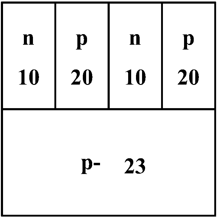
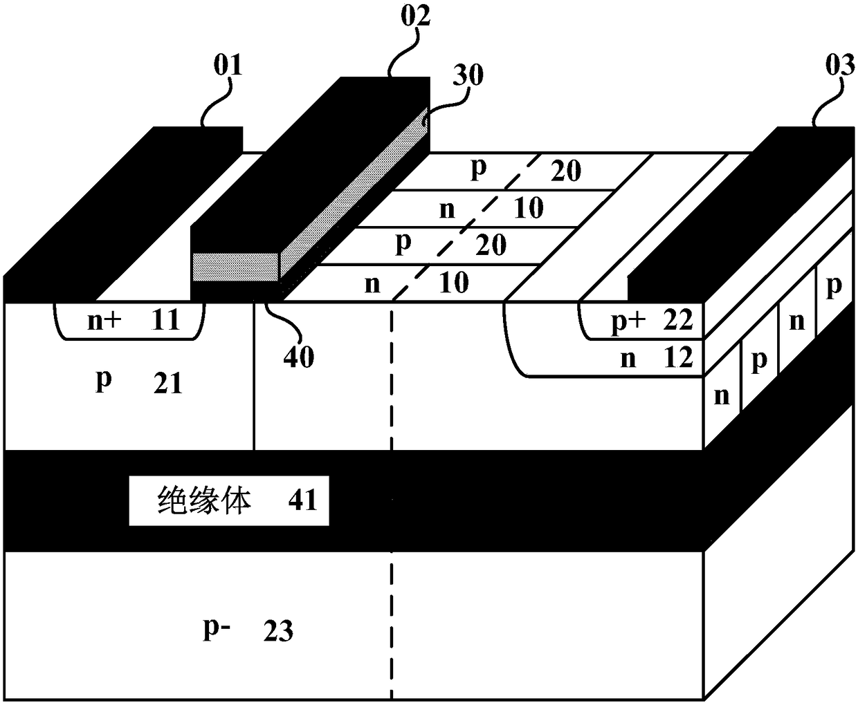
The invention discloses a high-speed superjunction lateral insulated gate bipolar translator, and belongs to the technical field of a semiconductor power device. Rapid breaking is achieved by replacing a light-doped substrate of an existing bulk silicon superjunction lateral insulated gate bipolar translator to a heavily-doped substrate, the breakdown voltage of the device is ensured by reasonablysetting impurity total number of each drift region in a superjunction voltage-resistant layer, and the application of the high-speed superjunction lateral insulated gate bipolar translator in an integrated circuit is achieved by further arranging a semiconductor second substrate region and a semiconductor isolation region. By the high-speed superjunction lateral insulated gate bipolar translator,the conflict between cost and rapid breaking on a bulk silicon substrate of the superjunction lateral insulated gate bipolar translator is solved.

Description

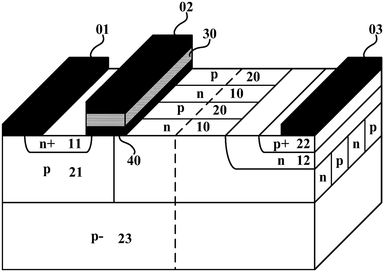
technical field [0001] The invention belongs to the technical field of semiconductor power devices, and in particular relates to a high-speed super-junction lateral insulated gate bipolar transistor. Background technique [0002] In a superjunction lateral insulated gate field effect transistor (LIGBT: Lateral Insulated Gate Bipolar Translator), electrons and holes participate in conduction at the same time, and these two types of carriers form conductance modulation, which greatly reduces the specific on-resistance of the device and reduces The chip area occupied by the device is taken into account. For its typical structure, refer to the transistor structure shown in Figure 1. However, in devices based on bulk silicon substrates, carriers will enter the lightly doped substrate, forming non-equilibrium carriers. In this way, when the device is turned off, it takes a certain time to extract these carriers, which prolongs the turn-off time and increases the turn-off power co...

Claims


Application Information

Patent Timeline
IPC IPC(8): H01L29/739H01L29/06H01L29/10H01L29/36
CPCH01L29/0634H01L29/10H01L29/36H01L29/7393H01L29/7394H01L29/66325H01L29/0834H01L29/1095H01L29/0808H01L29/0821H01L29/0619
Inventor 林智袁琦韩姝胡盛东周建林唐枋周喜川
Owner CHONGQING UNIV
Why Eureka
Try Eureka