Semiconductor wafer hole manufacturing method

A manufacturing method and semiconductor technology, applied in semiconductor/solid-state device manufacturing, electrical components, circuits, etc., can solve the problems of prolonging etching time, difficult photolithography, wafer damage, etc., and achieve the effect of prolonging etching time

Active Publication Date: 2018-08-07
CHENGDU HIWAFER SEMICON CO LTD
View PDF10 Cites 0 Cited by
  • Summary
  • Abstract
  • Description
  • Claims
  • Application Information

AI Technical Summary

Problems solved by technology

In response to the above requirements, two processes are usually used: one is to etch two kinds of blind holes twice, because the depth of blind holes is generally tens or even hundreds of microns, which makes the second photolithography difficult and poor in stability; The second is to use one-time photolithography. In this way, when the depths of the two holes are different, the holes with the smaller depth often need to be further extended after the hole is formed; when the two holes have different sizes, the cross-sectional The etching rate of holes with a large area is slow, and often after the formation of holes with a small cross-sectional area, the holes with a large cross-sectional area do not meet the etching requirements, and the etching time needs to be further extended; it can be seen that the two methods of the second method In both cases, it is necessary to extend the etching time, which will cause the depth of the hole formed by etching faster to be greater than the preset value, reduce the precision of the wafer, and even cause damage to the wafer

Method used


Image

  • Semiconductor wafer hole manufacturing method
  • Semiconductor wafer hole manufacturing method
  • Semiconductor wafer hole manufacturing method

Examples


Embodiment Construction

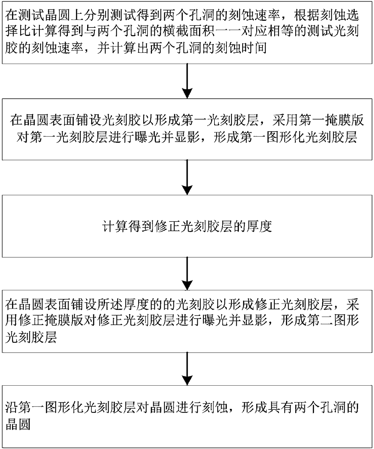
[0022] In order to make the purpose, technical solution and advantages of the present application clearer, the present application will be further described in detail below in conjunction with the accompanying drawings and specific embodiments. For simplicity, some technical features known to those skilled in the art are omitted from the following description.

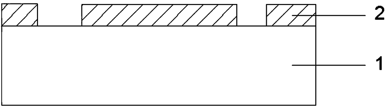
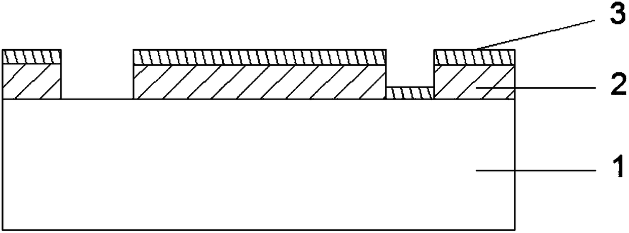
[0023] Such as Figure 1-5 As shown, the present embodiment provides a semiconductor wafer hole manufacturing method, including:

[0024] Basic parameter calculation steps:

[0025] Separately test 2 holes to be etched on the same test wafer as the product wafer, that is, measure the etching time required for each hole when etching the same depth, and divide the depth value by the etching of each hole time so as to obtain the etching rate E of the first hole 4 and the second hole 5 1 ,E 2 According to the etching selection ratio of the test wafer 1 and the test photoresist, the etching rate E of the photoresist cor...


PUM


Abstract

The invention relates to the radio frequency microwave semiconductor making technology field and particularly relates to a semiconductor wafer hole manufacturing method. The method comprises steps that etching rates of two holes are acquired through the test on a test wafer, and the equal etching rate of the test photoresist and the etching time of the two holes in one-to-one correspondence with cross-sectional areas of the two holes are acquired through calculation; a first photoresist layer is laid on a surface of a wafer, the first photoresist layer is exposed and developed to form a firstgraphic photoresist layer; thickness of the correction photoresist layer is acquired through calculation; the correction photoresist layer with the thickness is laid on the surface of the wafer, and the correction photoresist layer is exposed and developed to form a second graphic photoresist layer; the wafer is etched along the first graphic photoresist layer, and the wafer having the two holes is formed. The method is advantaged in that the relatively long etching time is taken as reference, the etching time of another hole is extended through laying the correction photoresist layer, and theetching depth beyond a preset value or damage to the wafer is avoided.

Description

technical field [0001] The invention belongs to the technical field of semiconductor manufacturing, and in particular relates to a method for manufacturing holes in semiconductor wafers. Background technique [0002] With the continuous expansion of new semiconductor applications, many traditional semiconductor processes can no longer meet the needs of product production, among which the semiconductor wafer hole manufacturing process is particularly prominent. [0003] In the RF-MEMS process, due to the need for impedance matching, it is often necessary to make blind holes of two different sizes or two different depths on the Si wafer. In response to the above requirements, two processes are usually used: one is to etch two kinds of blind holes twice, because the depth of blind holes is generally tens or even hundreds of microns, which makes the second photolithography difficult and poor in stability; The second is to use one-time photolithography. In this way, when the dep...

Claims


Application Information

Patent Timeline
Patent Type & Authority Applications(China)
IPC IPC(8): H01L21/027
CPCH01L21/027
Inventor 陈一峰
Owner CHENGDU HIWAFER SEMICON CO LTD
Why Eureka
Try Eureka