A display panel and method of making the same

A display panel and display area technology, which is applied in the direction of identification devices, instruments, semiconductor devices, etc., can solve the problems of increasing the cost of the mask, abnormal display, easy to break, etc., and achieve the effect of saving the cost of the mask and prolonging the etching time

Active Publication Date: 2022-07-12
WUHAN CHINA STAR OPTOELECTRONICS SEMICON DISPLAY TECH CO LTD
View PDF4 Cites 0 Cited by
  • Summary
  • Abstract
  • Description
  • Claims
  • Application Information

AI Technical Summary

Problems solved by technology

[0005] At present, flexible display devices are prone to fracture after repeated bending, resulting in abnormal display; in order to improve the bending characteristics of the display panel, an anti-fracture design will be added in the display area and bending area; generally, holes are punched in the inorganic layer And fill organic materials to form a flexible organic layer, but the new anti-fracture design will increase the cost of the photomask, so it is necessary to find a new type of display panel and its preparation method to solve the above problems

Method used


Image

  • A display panel and method of making the same
  • A display panel and method of making the same
  • A display panel and method of making the same

Examples


Embodiment 1

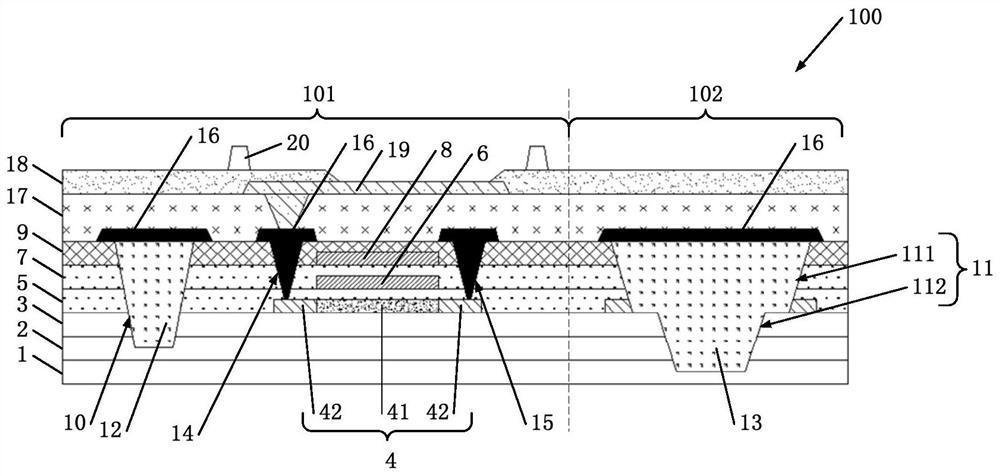
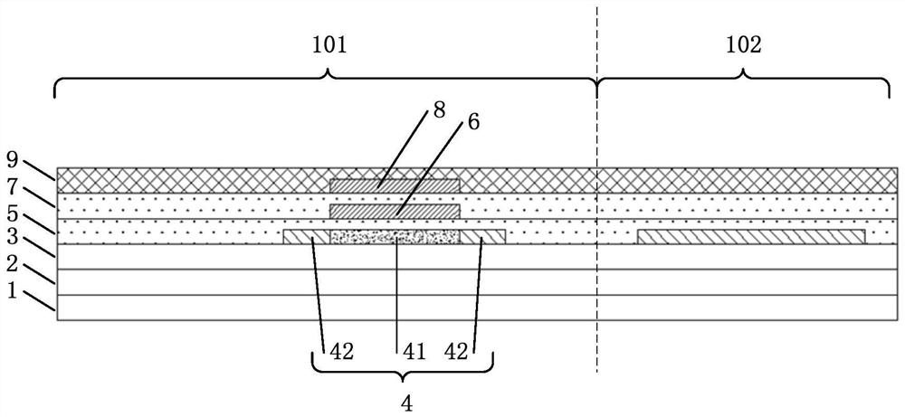
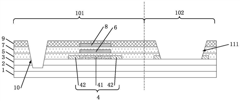
[0043] like figure 1As shown, a display panel 100 is defined with a display area 101 and a non-display area 102, and the non-display area 102 has a bending area. The display panel 100 includes: a substrate 1 , a barrier layer 2 , a buffer layer 3 , an active layer 4 , a first gate insulating layer 5 , a first gate layer 6 , a second gate insulating layer 7 , and a second gate Polar layer 8 and interlayer insulating layer 9 .

[0044] like figure 1 As shown, the substrate 1 may include a first substrate, an intermediate layer and a second substrate. Wherein, the constituent materials of the first substrate and the second substrate can be selected from polyimide, and the first substrate and the second substrate made by this can have good flexibility. The composition material of the intermediate layer can be SiO2 or SiNx, or can be a laminated structure of SiO2 and SiNx. The intermediate layer prepared by this has good water and oxygen resistance, and can also improve the perf...

Embodiment 2

[0058] This embodiment provides a manufacturing method for manufacturing the display panel 100 involved in the present invention.

[0059] like figure 2 As shown, in S1, a substrate 1 is provided, and the display panel 100 to be prepared is defined into a display area 101 and a non-display area 102, and the non-display area 102 has a bending area; S2, barriers are sequentially prepared on the substrate 1 Layer 2 , buffer layer 3 , active layer 4 , interlayer insulating layer 9 .

[0060] like figure 2 As shown, the active layer 4 is disposed on the display area 101 and the buffer layer 3 in the bending area. Since the depth of the first groove 10 is greater than the thickness of the first groove body 111 of the second groove 11, and the etching rate of the active layer 4 is slower than that of the film layer disposed thereon, the buffer layer in the bending region is The active layer 4 is provided on the 3 , so that the first mask can meet the depth requirements of the fi...


PUM


Abstract

The present invention relates to a display panel and a preparation method thereof. In the present invention, a first groove is formed in the display area from the surface of the interlayer insulating layer in the display area away from the substrate to the barrier layer and from the curved surface through the first mask at the same time. The surface of the interlayer insulating layer of the folded region away from the substrate penetrates to the first groove body of the second groove in the active layer, which saves the cost of the mask. On the other hand, the present invention retains the active layer in the bending area, thereby prolonging the etching time of the first groove body, so that the first mask can satisfy the depth of the first groove and the first groove of the second groove at the same time. body depth requirements.

Description

technical field [0001] The present invention relates to the field of display technology, in particular to a display panel and a preparation method thereof. Background technique [0002] The display device can convert the data of the computer into various characters, numbers, symbols or intuitive images for display, and can use input tools such as keyboards to input commands or data into the computer, and add, delete, and change the display at any time with the help of the hardware and software of the system. content. Display devices are classified into plasma, liquid crystal, light emitting diode, and cathode ray tube types according to the display device used. [0003] Organic light-emitting display devices (English full name: Organic Light-Emitting Diode, OLED for short) are also known as organic electric laser display devices and organic light-emitting semiconductors. The working principle of OLED is: when the power is supplied to an appropriate voltage, the positive ho...

Claims


Application Information

Patent Timeline
Patent Type & Authority Patents(China)
IPC IPC(8): H01L27/32G09F9/30
CPCG09F9/301H10K59/12H10K59/1201Y02E10/549
Inventor 杨薇薇
Owner WUHAN CHINA STAR OPTOELECTRONICS SEMICON DISPLAY TECH CO LTD
Why Eureka
Try Eureka