Convex point production method capable of preventing blue film

A fabrication method and bump technology, applied in semiconductor/solid-state device manufacturing, electrical components, electrical solid-state devices, etc., can solve problems such as difficulty in removing blue film, and easy contamination of bumps made of lead and tin materials.

Inactive Publication Date: 2008-09-24
SEMICON MFG INT (SHANGHAI) CORP +1
View PDF0 Cites 0 Cited by
  • Summary
  • Abstract
  • Description
  • Claims
  • Application Information

AI Technical Summary

Problems solved by technology

[0004] However, in the process of making the above bumps, the bumps made of lead and tin are easy to contaminate other areas other than the bumps, forming a blue film that is difficult to remove

Method used


Image

  • Convex point production method capable of preventing blue film
  • Convex point production method capable of preventing blue film
  • Convex point production method capable of preventing blue film

Examples


Embodiment Construction

[0020] Hereinafter, the method for manufacturing bumps that can avoid the blue film of the present invention will be further described in detail.

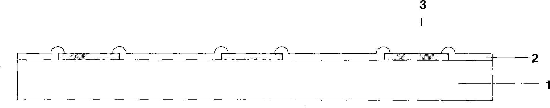
[0021] See figure 1 , Shows a cross-sectional view of a wafer using the present invention to avoid the blue film bump manufacturing method. As shown in the figure, a metal pad 2 and a passivation layer 3 are formed on the wafer 1.

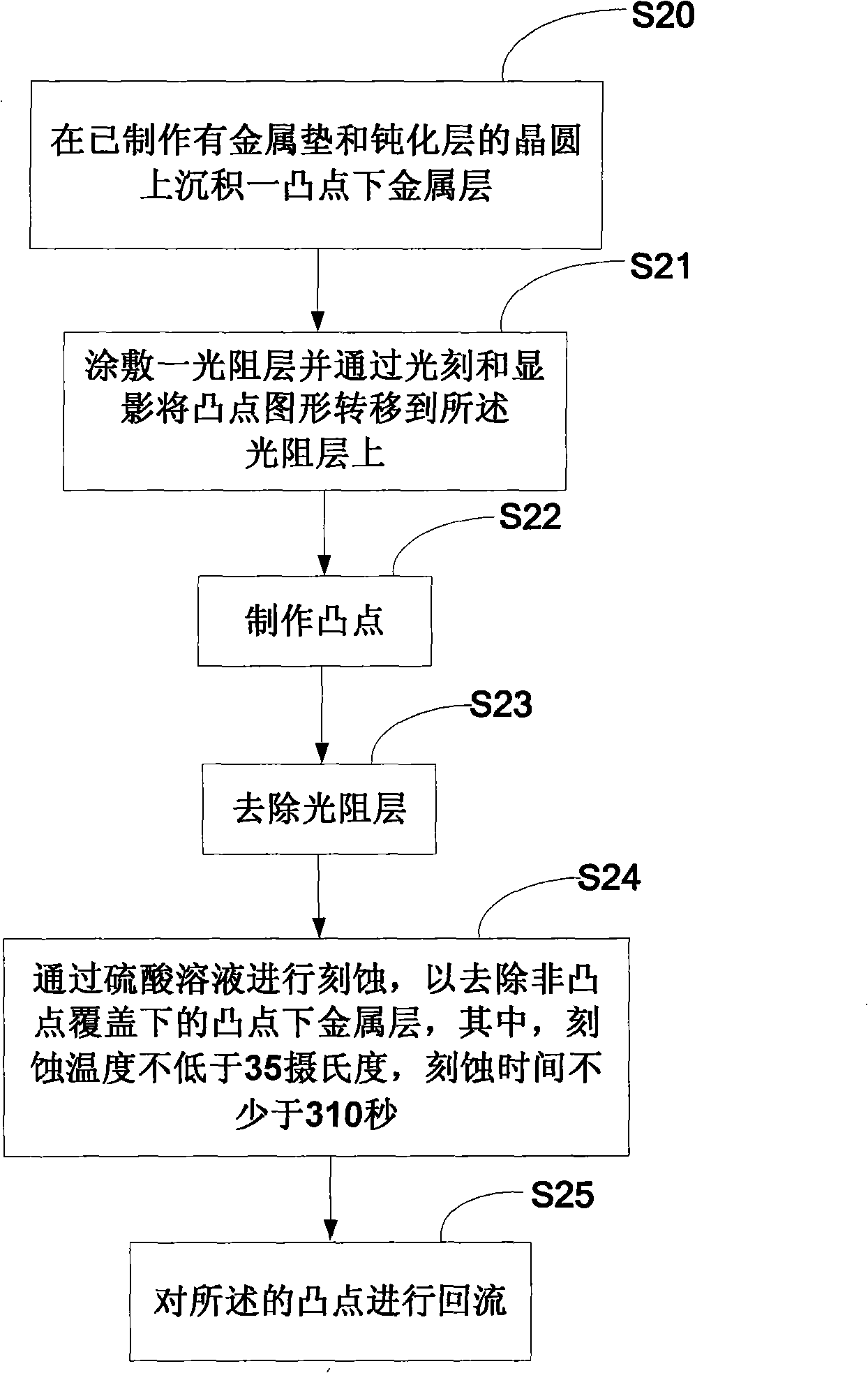
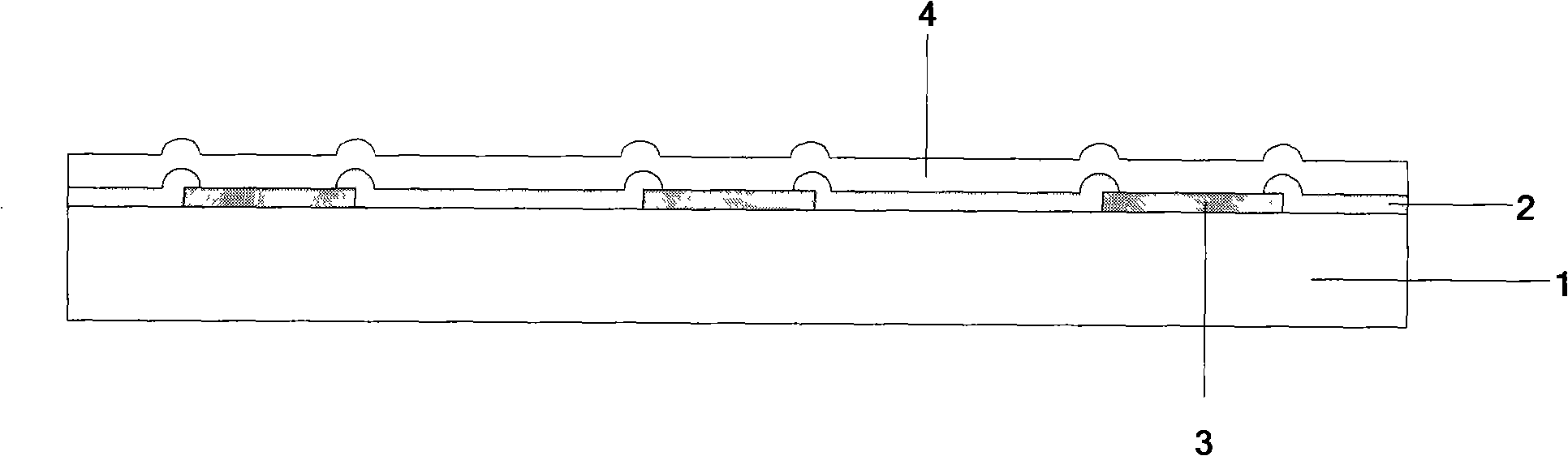
[0022] See figure 2 The method for manufacturing bumps that can avoid blue film of the present invention first proceeds to step S20 to deposit an under bump metal layer on the wafer on which the metal pad 2 and the passivation layer 3 have been fabricated. See image 3 , Showing the cross-sectional view of the wafer after step S20 is completed, refer to figure 1 As shown in the figure, the under-bump metal layer 4 is deposited on the metal pad 2 and the passivation layer 3.

[0023] Then continue to step S21, apply a photoresist layer and transfer the convex dot pattern to the photoresist layer by photol...


PUM


Abstract

The invention provides a convex point fabrication method which can avoid blue membrane appearance. The existing convex point fabrication method uses low-temperature sulfuric acid solution for carrying out the etching, so as to remove a metal layer below the convex point; the metal layer below the convex can be removed, but the blue membrane is easy to be generated. In the convex point fabrication method of the invention which can avoid the blue membrane appearance, a metal layer below the convex point is firstly deposited on the existing wafers with a metal pad and a passivation layer fabricated, a light resistance layer is plated on the metal layer and the convex point images are transferred on the light resistance layer by lithography and development; the convex point is then fabricated and the light resistance is removed then; the sulfuric acid solution is then used for carrying out the etching, so as to remove the metal layer below the convex point which is covered by non-convex point; the convex point is finally refluxed; wherein, in the step that the metal layer below the convex point under the coverage of non-convex point is removed by carrying out the etching with the sulfuric acid solution, the etching temperature is not lower than 35 DEG C and the etching time is not less than 310 seconds. Blue membranes can be avoided by adopting the method of the invention when the convex point is fabricated.

Description

Technical field [0001] The present invention relates to the field of semiconductor manufacturing, in particular to a method for manufacturing bumps that can avoid blue film. Background technique [0002] In order to meet the requirements of portable electronic products for short, small, light and thin components, bumps are made on the metal pads of the wafer chips as the lead-out ends, and then flip-chip soldering is performed directly. In order to save costs, the commonly used bumps are lead-tin bumps. [0003] The production of bumps usually includes the following steps: first deposit an under-bump metal layer on the wafer with metal pads and passivation layers, then apply a photoresist layer and transfer the bump pattern by photolithography and development On the photoresist, the bumps are then made, then the photoresist is removed, and then etched by sulfuric acid solution to remove the under bump metal layer under non-bump coverage, and finally the bumps are reflowed. In the...

Claims


Application Information

Patent Timeline
Patent Type & Authority Applications(China)
IPC IPC(8): H01L21/60
CPCH01L24/11H01L2224/03912H01L2224/0401H01L2224/05022H01L2224/05572H01L2224/11H01L2224/1147H01L2224/13H01L2924/00014H01L2924/00012
Inventor 孙支柱王重阳章剑名陈杰
Owner SEMICON MFG INT (SHANGHAI) CORP
Why Eureka
Try Eureka