Compound-eye imaging device

a compound-eye imaging and camera technology, applied in the field can solve the problems of affecting the degradation of each unit image, and the other problems so as to prevent the generation, improve the quality of compound-eye imaging devices, and avoid the effect of increasing the cost of manufacturing

Inactive Publication Date: 2010-04-20
FUNAI ELECTRIC CO LTD
View PDF9 Cites 50 Cited by
  • Summary
  • Abstract
  • Description
  • Claims
  • Application Information

AI Technical Summary

Benefits of technology

[0008]An object of the present invention is to provide a compound-eye imaging device which can prevent the generation of stray light without complicating the manufacturing process and increasing the cost thereof, and can obtain a good quality image without interference by the stray light.
[0009]This object is achieved according to the present invention by a compound-eye imaging device comprising: multiple optical lenses for collecting light in a capture zone; a solid-state imaging element for capturing, on a surface thereof, unit images formed by the multiple optical lenses, respectively; and a stray light blocking member provided on a capture zone side of the optical lenses for limiting an incident angle of light entering each optical lens for each unit image so as to prevent the light entering the each optical lens and emitted to the solid-state imaging element from interfering with other unit images than the each unit image.
[0010]The thus structured compound-eye imaging device of the present invention has the stray light blocking member provided on the capture zone side of the optical lenses, thereby eliminating the need to provide walls between the solid-state imaging element and the optical lenses, so that it can prevent the generation of stray light without complicating the manufacturing process and increasing the cost thereof, and can easily obtain a good quality image without interference by the stray light.
[0011]The compound-eye imaging device can further comprise a prism placed on the capture zone side of the optical lenses for changing propagation paths of lights to be collected on the optical lenses, wherein the stray light blocking member is placed on the capture zone side relative to the prism. Since the stray light blocking member is placed on the capture zone side relative to the prism, it can be mounted in the compound-eye imaging device without complicating the manufacturing process and increasing the cost thereof
[0012]The stray light blocking member can be a film attached to a surface of the prism or a layer printed on the prism. This makes it possible to further reduce the size of the entire compound-eye imaging device.

Problems solved by technology

However, a compound-eye imaging device having densely formed optical lenses to form unit images close to each other has a disadvantage that light entering through each optical lens to form each unit image corresponding to the each optical lens may interfere with light (hereafter referred to as “stray light”) entering through an adjacent optical lens or lenses, thereby degrading each unit image.
This may cause a combined image or a panoramic image produced from the unit images to be no good.
However, such compound-eye imaging device has other problems.
Thus, there is a problem that a complicated and time-consuming work is unavoidably required to accurately incorporate the walls into the narrow space, causing the manufacturing process of the compound-eye imaging device to be complicated.
However, this further complicates the manufacturing process and increases the cost of the compound-eye imaging device.

Method used


Image

  • Compound-eye imaging device
  • Compound-eye imaging device
  • Compound-eye imaging device

Examples


first embodiment

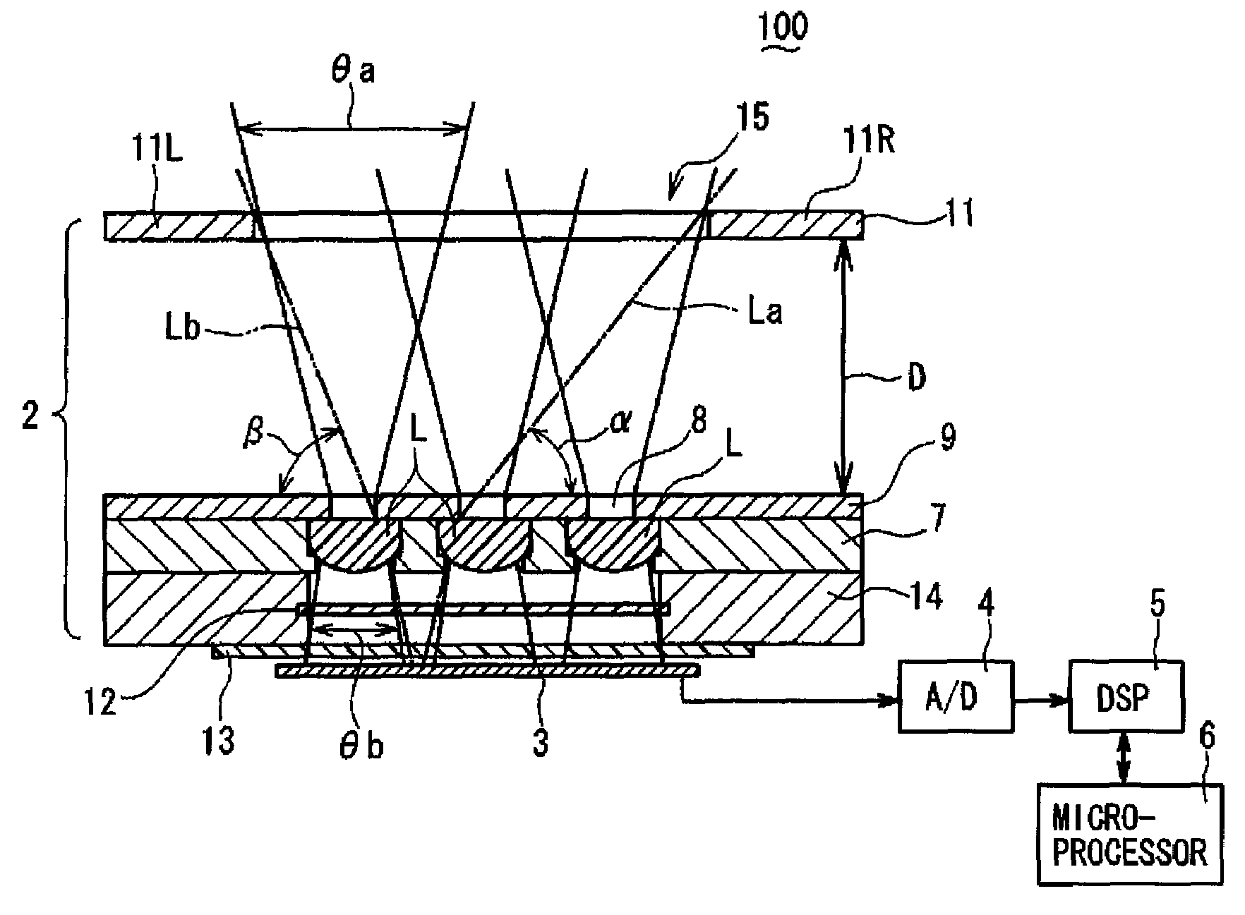
[0024]Referring to FIG. 1 to FIG. 3, a compound-eye imaging device 100 according to a first embodiment of the present invention will be described. FIG. 1 is a schematic cross-sectional view (along line X-X shown in FIG. 3) and FIG. 2 is a schematic perspective view of the compound-eye imaging device 100. As shown in FIG. 1, the compound-eye imaging device 100 comprises in a housing (not shown) thereof: an optical system 2 including optical lenses M, described later, for collecting light in a capture zone to form multiple unit images on a predetermined focal plane; and a solid-state imaging element 3 placed at the focal plane of the optical lens system 2 for converting the multiple unit images formed by the optical lens system 2 to electronic image information. The compound-eye imaging device 100 further comprises: an A / D (Analog-to-Digital) converter 4 for converting the electronic image information to digital information; a DSP (Digital Signal Processor) 5 for receiving the digital...

second embodiment

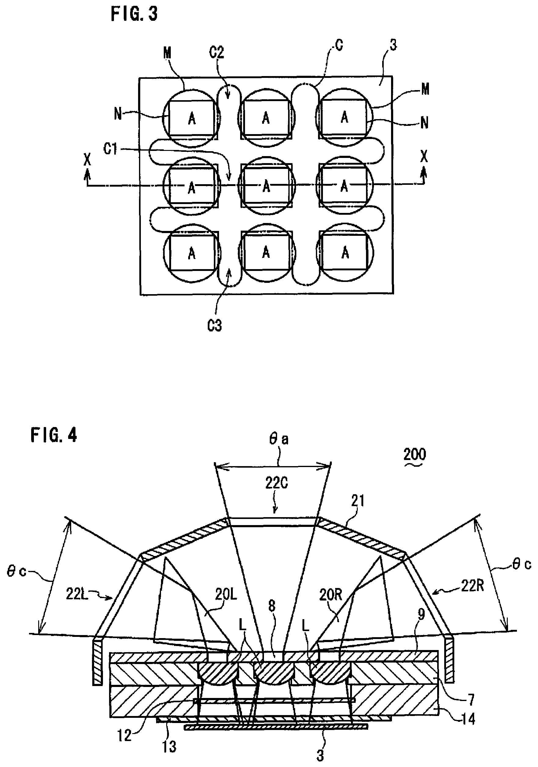
[0037]Referring to FIG. 4 and FIG. 5, a compound-eye imaging device 200 according to a second embodiment of the present invention will be described below. FIG. 4 is a schematic cross-sectional view and FIG. 5 is a schematic plan view of the compound-eye imaging device 200. The compound-eye imaging device 200 of the second embodiment has substantially the same structure as that of the compound-eye imaging device 100 of the first embodiment except for the following. First, in the compound-eye imaging device 200, the number of optical lenses L of an optical system 2 is three, in which the three optical lenses L are arranged in one row, left, center and right (refer to FIG. 5).

[0038]Second, 45-45-90 degree right-angle prisms 20L, 20R to change the propagation paths of lights to be collected on the respective optical lenses L are provided on the capture zone side of the left and right optical lenses L, respectively. Third, a stray light blocking member 21 has three windows 22L, 22C, 22R,...

third embodiment

[0041]Referring now to FIG. 6 and FIG. 7, a compound-eye imaging device 300 according to a third embodiment of the present invention will be described hereinafter. FIG. 6 is a schematic cross-sectional view and FIG. 7 is a schematic plan view of the compound-eye imaging device 300. The compound-eye imaging device 300 of the third embodiment has substantially the same structure as that of the compound-eye imaging device 200 of the second embodiment except for the following. First, in the compound-eye imaging device 300, three optical lenses L are not arranged in a row, but are arranged at the vertexes of a triangle as seen in plan view (refer to FIG. 7).

[0042]Second, each of the optical lenses L is set to have a view angle of about 40° (forty degrees), while left and right 45-45-90 degree right angle prisms 30L, 30R are set to have a mounting angle γ of about 25° (twenty-five) to the optical lenses L, respectively, so as to allow effective incident view angle ranges θc, θa, θc to con...


PUM


Abstract

A compound-eye imaging device comprises nine optical lenses arranged in a matrix array of three rows and three columns, and a solid-state imaging element for capturing unit images formed by the optical lenses. A stray light blocking member having a rectangular-shaped window is provided on the capture zone side of the optical lenses, eliminating the need to provide, between the solid-state imaging element and the optical lenses, walls by which light propagation paths of lights emitted from the optical lenses are partitioned from each other. The stray light blocking member blocks incident lights in a range outside each effective incident view angle range of each optical lens. This prevents the light entering each optical lens to form a unit image from interfering with other unit images formed by adjacent optical lenses, thereby obtaining a good quality image, without complicating the manufacturing process and increasing the cost thereof.

Description

BACKGROUND OF THE INVENTION[0001]1. Field of the Invention[0002]The present invention relates to a compound-eye imaging device.[0003]2. Description of the Related Art[0004]A compound-eye imaging device is known as an imaging device to realize a thin camera as disclosed, for example, in Japanese Laid-open Patent Publication Hei 10-84104. The compound-eye imaging device (image sensor) according to Japanese Laid-open Patent Publication Hei 10-84104 has a lenslet array of multiple integrated optical lenses (lenslets), and a solid-state imaging element (photosensor array) for capturing multiple unit images formed by the optical lenses.[0005]Generally, in order to reduce the size of the compound-eye imaging device, the optical lenses are densely formed, and the unit images formed by the optical lenses are also formed close to each other on the solid-state imaging element. However, a compound-eye imaging device having densely formed optical lenses to form unit images close to each other ha...

Claims


Application Information

Patent Timeline
Patent Type & Authority Patents(United States)
IPC IPC(8): H04N101/00H04N5/335H04N5/225H01L27/00G03B15/00H04N5/357
CPCH04N5/2254H04N23/55
Inventor TOYODA, TAKASHINAKAO, YOSHIZUMIKUGO, KOUICHIMASAKI, YASUO
Owner FUNAI ELECTRIC CO LTD
Why Eureka
Try Eureka