Package structure of micro LED display module

A display module and packaging structure technology, applied in electrical components, electrical solid-state devices, circuits, etc., can solve the problem that the resolution of the display screen cannot be further improved, and achieve the effect of improving color stability, improving display resolution, and reducing size

Inactive Publication Date: 2018-08-14
JIANGSU WENRUN OPTOELECTRONICS
View PDF0 Cites 12 Cited by
  • Summary
  • Abstract
  • Description
  • Claims
  • Application Information

AI Technical Summary

Problems solved by technology

Among them, SMD LED devices are all packaged in the way of front-mounted chips. Due to the limitations of front-mounted chip packaging, the package size of SMD LEDs in the current market is close to the limit, and it is difficult to further reduce the size of the device and improve the resolution of the display screen; The method of surface-mounting the chip device to the circuit board is limited by the circuit board and the SMT process, and there is a large gap between the LEDs, which also makes the resolution of the display screen unable to be further improved.

Method used


Image

  • Package structure of micro LED display module
  • Package structure of micro LED display module
  • Package structure of micro LED display module

Examples


Embodiment Construction

[0023] Below in conjunction with accompanying drawing, technical scheme of the present invention is described in further detail:

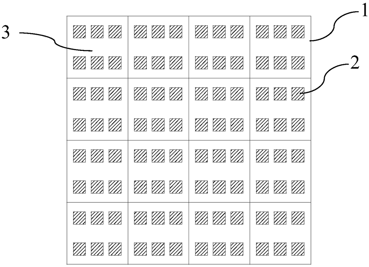
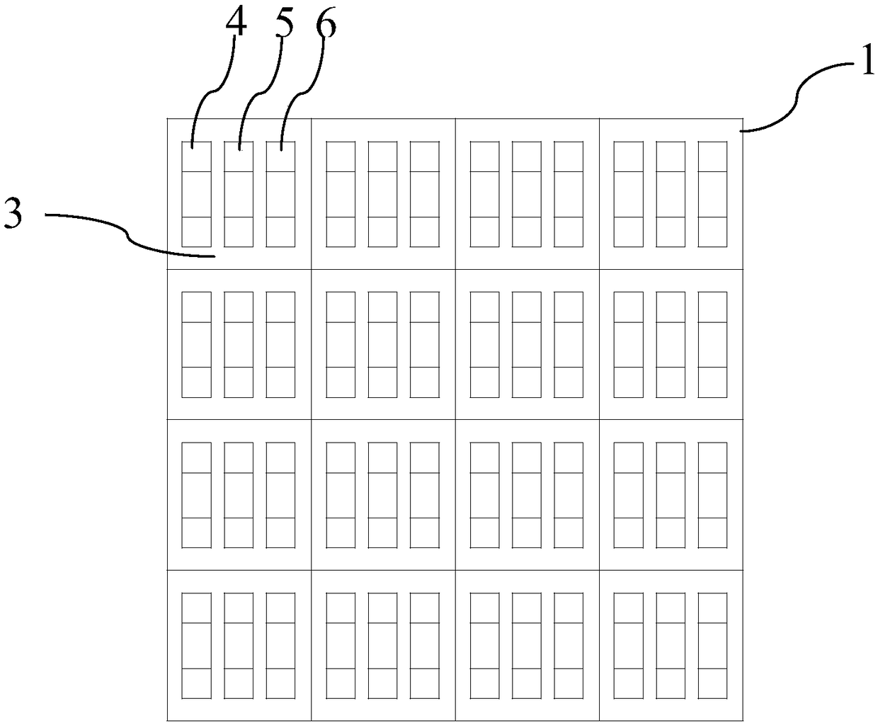
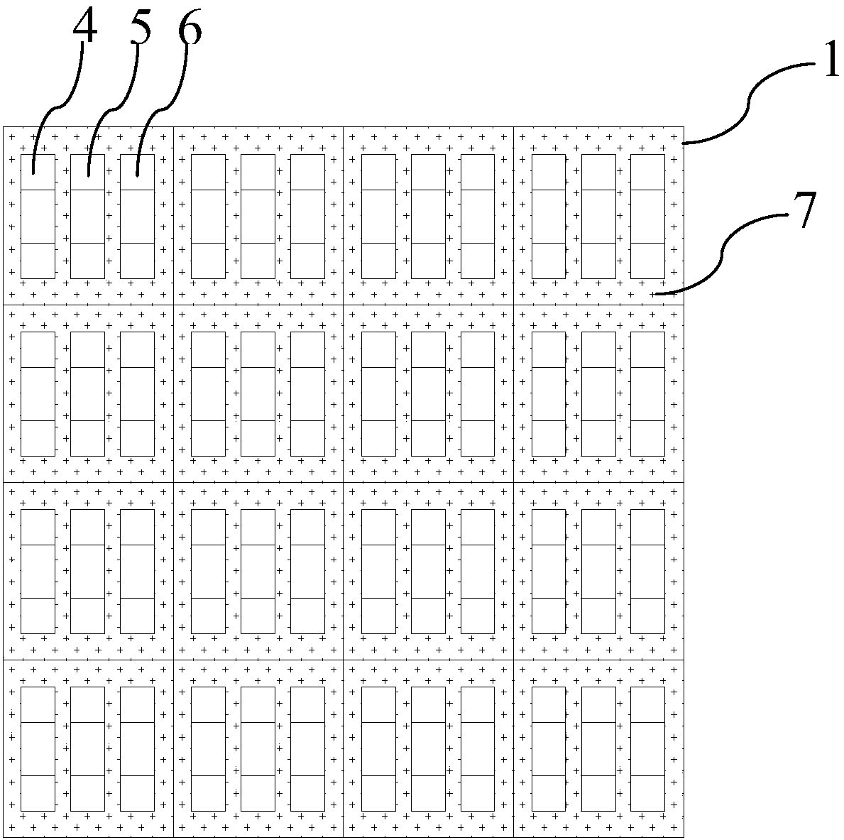
[0024] Such as figure 1 Prepare display module circuit board 1, figure 2 The first flip-chip blue light chip 4, the flip-chip green light chip 5, and the second flip-chip blue light chip 6 are fixed to the corresponding electrodes of the circuit board by flip-chip technology, image 3 The filling layer 7 is used to fill the gap between the chips, Figure 4 A red fluorescent layer 8 is coated on the surface of the second flip-chip blue light chip 6, so that after the blue light chip emits light, it is excited by the red fluorescent layer to fully absorb and emit red light. Figure 5 The entire surface of the module is encapsulated with a transparent encapsulation layer to protect the internal structure of the module and complete the encapsulation of a micro LED display module.

[0025] Image 6 It is a schematic cross-sectional view of an LED d...


PUM


Abstract

The invention discloses a package structure of a micro LED display module. The package structure comprises a circuit board, multiple light-emitting units, and a transparent package layer; each light-emitting unit comprises a first flip blue-light chip, a flip green-light chip and a second flip blue-light chip; the first flip blue-light chip, the flip green-light chip and the second flip blue-lightchip are orderly fixed on the circuit board, the gaps between the light-emitting units, between the first flip blue-light chip and the flip green-light chip, and between the flip green-light chip andthe second flip blue-light chip are filled by using filing layers; a red fluorescent layer is coated on the first flip blue-light chip or the second flip blue-light chip; and the transparent packagelayer wraps the whole surface of the circuit board and the light-emitting units. The package structure disclosed by the invention reduces the gaps among the LED particles when a surface mount device is in mounting, the single light-emitting unit size is greatly reduced to the micron order, the light-emitting unit density is improved, and the final display resolution is improved; and the problem ofthe thermal drift color aberration of the display screen is improved.

Description

technical field [0001] The invention relates to the technical field of LED packaging, in particular to a packaging structure of a miniature LED display module. Background technique [0002] At present, outdoor display screens on the market mainly use full-color LED SMD devices, and multiple full-color LED devices are surface-mounted on the circuit board to form a full-color LED array, and finally play the role of outdoor display. Among them, SMD LED devices are packaged in the way of front-mounted chips. Due to the limitations of front-mounted chip packaging, the size of SMD LED packages in the current market is close to the limit, and it is difficult to further reduce the size of the device and improve the resolution of the display screen; The method of surface-mounting the chip device to the circuit board is limited by the circuit board and the SMT process, and there is a large gap between the LEDs, which also makes the resolution of the display screen unable to be further...

Claims


Application Information

Patent Timeline
Patent Type & Authority Applications(China)
IPC IPC(8): H01L33/48H01L33/56H01L33/50H01L25/075
CPCH01L33/486H01L25/0753H01L33/502H01L33/56H01L2933/0033H01L2933/0041H01L2933/005
Inventor 严春伟
Owner JIANGSU WENRUN OPTOELECTRONICS
Why Eureka
Try Eureka