
Magnetic thin film inductor structures

A magnetic thin film and inductor technology, applied in the direction of inductors, transformer/inductor cores, electric solid devices, etc.

Inactive Publication Date: 2018-08-21
TAIWAN SEMICON MFG CO LTD
View PDF0 Cites 0 Cited by
  • Summary
  • Abstract
  • Description
  • Claims
  • Application Information

AI Technical Summary

Problems solved by technology

However, with each advance in the semiconductor fabrication process, new challenges have been discovered in creating integrated circuits
[0003] One such challenge involves making inductors with newer semiconductor process technologies

Method used


Image

  • Magnetic thin film inductor structures
  • Magnetic thin film inductor structures
  • Magnetic thin film inductor structures

Examples


Embodiment approach

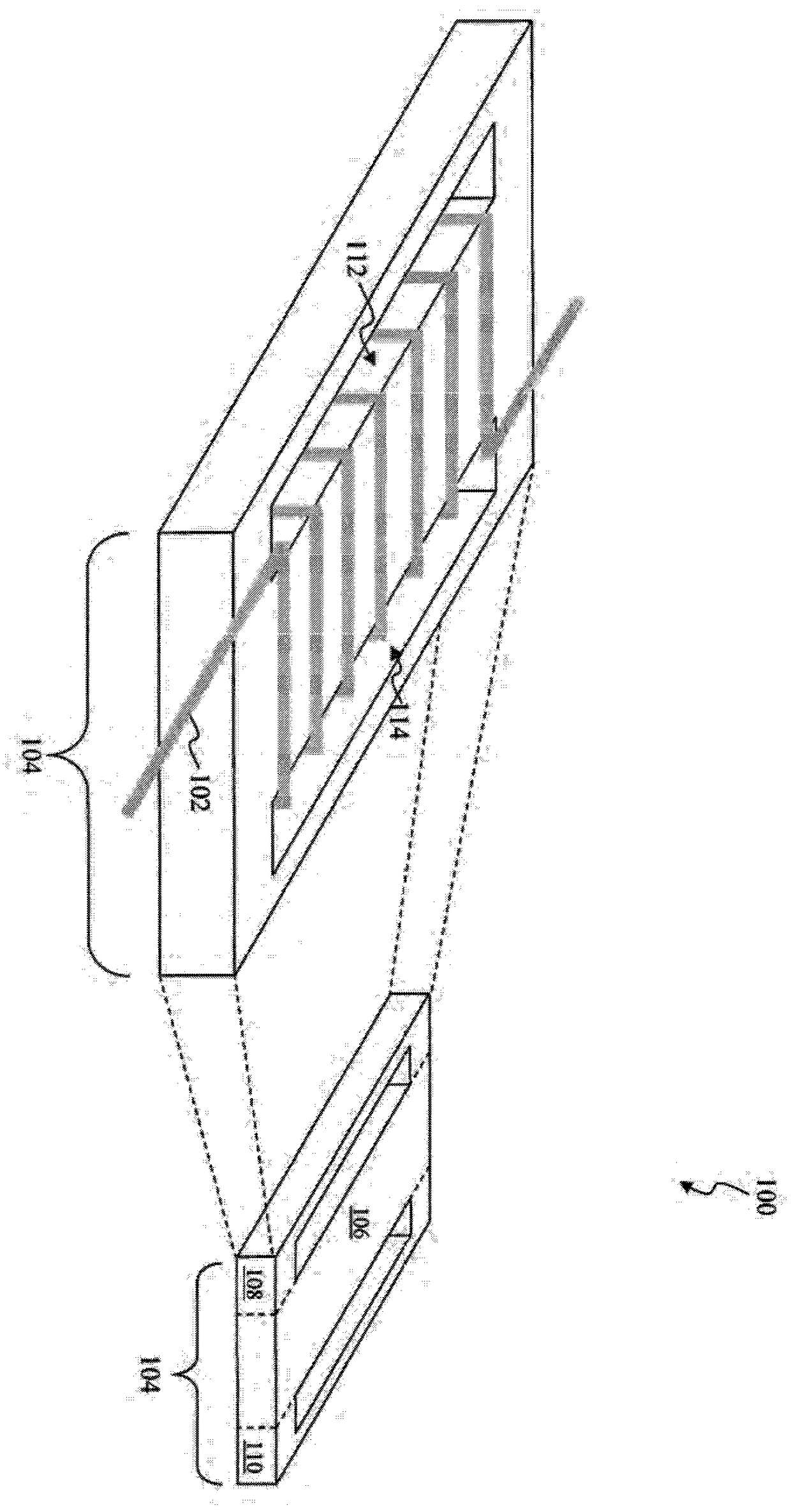
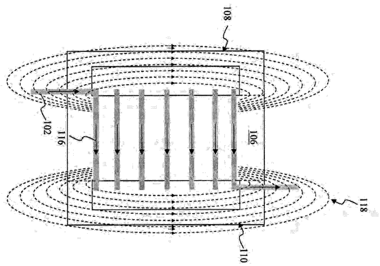
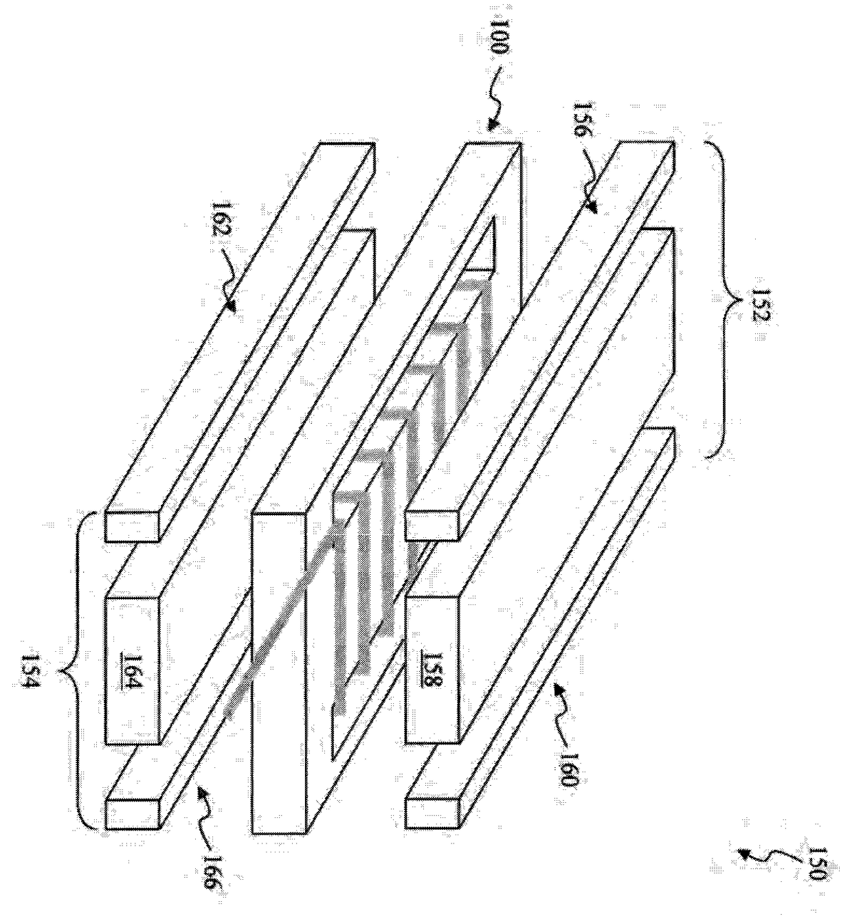
[0032] Although in Figure 1C The first magnetic thin film planar structure 152 and the second magnetic thin film planar structure 154 are described as rectangular parallelepipeds, but those skilled in the art will recognize that the Other embodiments: such as one or more three-dimensional regular closed geometric structures, such as for example one or more three-dimensional regular polygons; one or more three-dimensional irregular closed structures, such as for example one or more three-dimensional irregular polygons; and / or any suitable combination of these closed structures. In an exemplary embodiment, the first magnetic thin film planar structure 152 and / or the second magnetic thin film planar structure 154 can be utilized as described above in Figure 1A The magnetic thin film material and / or the parallel magnetic thin film material described in are implemented. In some cases, the magnetic thin film material can be as above in Figure 1A Depositing on one or more ferroma...


PUM


Abstract

Various magnetic thin film inductor structures are disclosed that include one or more magnetic thin film (MTF) materials. During operation, an electric field passes through one or mare conductive windings which, in turn, generates a magnetic field for storing energy within these magnetic thin film inductor structures. The magnetic thin film (MTF) materials within these magnetic thin film inductorstructures effectively attract magnetic flux lines of this magnetic field. As a result, any magnetic leakage resulting from the magnetic field generated by these magnetic thin film inductor structuresonto nearby electrical, mechanical, and / or electro-mechanical devices is lessened when compared to magnetic leakage resulting from the magnetic field generated by other inductor structures not havingthe one or more MTF materials.

Description

technical field [0001] Embodiments of the present invention relate to a magnetic film inductor structure. Background technique [0002] Continuous advances in semiconductor fabrication processes have enabled manufacturers and designers to create smaller and more powerful electronic devices. The manufacturing of semiconductor devices has developed from the 10-micron semiconductor manufacturing process achieved around 1971 to the 22-nanometer semiconductor manufacturing process achieved around 2012. It is expected that the fabrication of semiconductor devices will further develop to a 5nm semiconductor fabrication process around 2019. With each advance in semiconductor fabrication processes, the components of integrated circuits have become smaller to enable more components to be fabricated on a semiconductor substrate. However, with each advance in semiconductor fabrication processes, new challenges have been discovered in creating integrated circuits. [0003] One such ch...

Claims


Application Information

Patent Timeline
IPC IPC(8): H01L49/02H01F27/24H01F27/28
CPCH01F27/24H01F27/28H01L28/10
Inventor 艾伦罗斯艾力克苏宁保罗拉努奇
Owner TAIWAN SEMICON MFG CO LTD
Learn More