
A preparation method of a low activation voltage resistive switch device

A technology for activating voltage and resistive switching devices, which is applied in the field of information storage, can solve the problems of unsatisfactory resistive storage characteristics, lack of resistive switching characteristics, and high defect formation energy, and achieve easy repeatable tests, low equipment requirements, and lower activation voltage Effect

Active Publication Date: 2020-02-14
SUN YAT SEN UNIV
View PDF5 Cites 0 Cited by
  • Summary
  • Abstract
  • Description
  • Claims
  • Application Information

AI Technical Summary

Problems solved by technology

It is found in the research that the dielectric layer materials with low defect formation energy often have unsatisfactory resistive switching storage properties, or even do not have resistive switching properties.
The dielectric layer material with better storage properties often has higher defect formation energy.

Method used

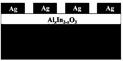
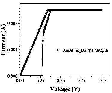
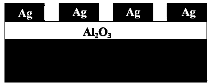

Image

  • A preparation method of a low activation voltage resistive switch device
  • A preparation method of a low activation voltage resistive switch device
  • A preparation method of a low activation voltage resistive switch device

Examples


Embodiment 1

[0030] Pt / Ti / SiO with a length of 1 cm and a width of 1 cm 2 / Si substrates were cleaned with acetone, isopropanol, and deionized water, and dried for later use.

[0031] Prepare 0.2 mol / L indium nitrate aqueous solution and stir for 24 h before use.

[0032] A certain amount of solid aluminum nitrate was weighed and dissolved in 2.5 ml of hydrogen peroxide (30%) to prepare a 0.2 mol / L aluminum nitrate solution.

[0033] Add 111 μL of ammonia water and 75 μL of nitric acid to the aluminum nitrate solution, and stir for 24 h to obtain a mixed solution of aluminum nitrate.

[0034] Indium nitrate aqueous solution was spin-coated on Pt / Ti / SiO 2 / Si substrate, and then heated on a hot plate for 5 min. This process was repeated 4 times. The samples were then annealed in an annealing furnace at 180 °C for 1 h, and then allowed to cool naturally to room temperature.

[0035] After the sample was taken out, the aluminum nitrate mixed solution was spin-coated on the sample, and th...

Embodiment 2

[0040] Pt / Ti / SiO with a length of 1 cm and a width of 1 cm 2 / Si substrates were cleaned with acetone, isopropanol, and deionized water, and dried for later use.

[0041] Prepare 0.22 mol / L indium nitrate aqueous solution and stir for 24 h before use.

[0042] A certain amount of solid aluminum nitrate was weighed and dissolved in 2.5 ml of hydrogen peroxide (30%) to prepare a 0.18 mol / L aluminum nitrate solution.

[0043]Add 111 μL of ammonia water and 75 μL of nitric acid to the aluminum nitrate solution, and stir for 24 h to obtain a mixed solution of aluminum nitrate.

[0044] Indium nitrate aqueous solution was spin-coated on Pt / Ti / SiO 2 / Si substrate, and then heated on a hot plate for 5 min. This process was repeated 4 times. The samples were then annealed in an annealing furnace at 150 °C for 1 h, and then allowed to cool down to room temperature naturally.

[0045] After the sample was taken out, the aluminum nitrate mixed solution was spin-coated on the sample, ...

Embodiment 3

[0049] Pt / Ti / SiO with a length of 1 cm and a width of 1 cm 2 / Si substrates were cleaned with acetone, isopropanol, and deionized water, and dried for later use.

[0050] Prepare 0.22 mol / L indium nitrate aqueous solution and stir for 24 h before use.

[0051] A certain amount of solid aluminum nitrate was weighed and dissolved in 2.5 ml of hydrogen peroxide (30%) to prepare a 0.2 mol / L aluminum nitrate solution.

[0052] Add 111 μL of ammonia water and 75 μL of nitric acid to the aluminum nitrate solution, and stir for 24 h to obtain a mixed solution of aluminum nitrate.

[0053] Indium nitrate aqueous solution was spin-coated on Pt / Ti / SiO 2 / Si substrate, and then heated on a hot plate for 5 min. This process was repeated 4 times. The samples were then annealed in an annealing furnace at 180 °C for 1 h, and then allowed to cool naturally to room temperature.

[0054] After the sample was taken out, the aluminum nitrate mixed solution was spin-coated on the sample, and t...


PUM

PropertyMeasurementUnit
thicknessaaaaaaaaaa
pore sizeaaaaaaaaaa
thicknessaaaaaaaaaa

Abstract

The invention relates to the technical field of information storage, and more specifically, to a method for preparing a low activation voltage resistive switch device. The main steps are: 1) cleaning and pre-treating the surface of the conductive substrate for use; 2) subsequently growing on the conductive substrate and heat-treating to obtain the dielectric layer S1; 3) preparing the precursor solution A2 of the dielectric layer S2 , and add etchant to obtain the mixed precursor solution A3; 4) spin-coat the mixed precursor solution A3 on the dielectric layer S1 and heat-treat to obtain the composite dielectric layer S2(1) / S1; 5) in the composite dielectric layer S2(1) / S1 The top electrode is vapor-deposited on S1 to complete the preparation. The invention is easy to implement, has good repeatability and low cost, and can prepare a resistive variable device with low activation voltage under relatively low temperature and normal pressure conditions. This invention provides a new approach for the design and performance optimization of new semiconductor memory devices, and has important prospects in the electrical modification and directional regulation of semiconductor materials.

Description

technical field [0001] The invention relates to the technical field of information storage, and more specifically, to a method for preparing a low activation voltage resistive switch device. Background technique [0002] As a series of products such as mobile phones and tablet computers become more and more popular in our lives, portable electronic products receive more and more attention, and the corresponding market is also unprecedentedly huge. Among them, memory, as the core component of electronic products, plays a very important role in the performance of devices. However, limited by the transistor integration technology and the bottleneck of miniaturization, the current mainstream product flash memory (Flash) in the current market can no longer meet the demand of the market and the semiconductor industry for memory. Therefore, in recent years, many researchers at home and abroad have carried out many researches on next-generation memory. [0003] Resistive memory is...

Claims


Application Information

Patent Timeline
Patent Type & Authority Patents(China)
IPC IPC(8): H01L45/00
CPCH10N70/24H10N70/021H10N70/041H10N70/011
Inventor 段伟杰裴艳丽饶畅
Owner SUN YAT SEN UNIV
Learn More