Pixel circuit and image sensor device

An image sensor and pixel circuit technology, applied in image communication, television, electrical components, etc., can solve problems such as large parasitic capacitance, lower maximum sensitivity, and limit normal use of low-light scenes, so as to improve conversion gain and sensitivity, and improve pixel Quality, the effect of preventing signal overflow

Pending Publication Date: 2018-09-04
思特威(上海)电子科技股份有限公司
View PDF14 Cites 4 Cited by
  • Summary
  • Abstract
  • Description
  • Claims
  • Application Information

AI Technical Summary

Problems solved by technology

This will bring other problems, such as the parasitic capacitance of the floating diffusion point will be relatively large, the conversion gain will not be very high, and the maximum sensitivity will be reduced, thus limiting the normal use in low-light scenes

Method used


Image

  • Pixel circuit and image sensor device
  • Pixel circuit and image sensor device
  • Pixel circuit and image sensor device

Examples


Embodiment Construction

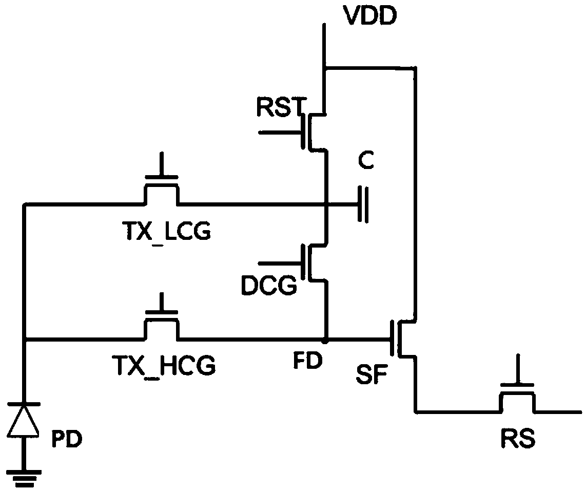
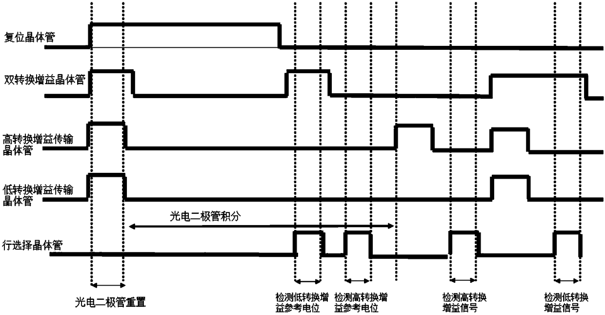
[0025] The content proposed by the present invention will be described in detail below in conjunction with the accompanying drawings. figure 2 It is a structural diagram of a pixel circuit proposed in Embodiment 1 of the present invention, image 3 It is a timing diagram of the pixel circuit of the first embodiment.

[0026] Such as figure 2 As shown in , the high conversion gain transfer transistor TX_HCG and the low conversion gain transfer transistor TX_LCG are respectively connected to the photodiode PD, and transfer and output the electrons generated by the photoelectric effect of the photodiode PD for the incident light. The high conversion gain pass transistor TX_HCG is connected to the floating diffusion FD, and the low conversion gain pass transistor TX_LCG is connected to the connection point of the reset transistor RST and the dual conversion gain transistor DCG. Capacitor C may be a device capacitance or a parasitic capacitance at the connection point of reset ...


PUM


Abstract

The invention provides a pixel circuit. The pixel circuit employs a plurality of transmission transistors: a high conversion gain transmission transistor and one or more low conversion gain transmission transistors. The pixel circuit comprises a reset transistor, a double-conversion-gain transistor, a capacitor, the high conversion gain transmission transistor, the low conversion gain transmissiontransistor and an output unit. The output unit comprises an amplification transistor and a row selection transistor. The pixel circuit further comprises an anti-overflow transistor for controlling afull-well signal. The one or more low conversion gain transmission transistors form one or more transmission branches, which are respectively connected to a photodiode. The plurality of low conversiongain transmission transistors can be respectively connected to a plurality of transmission branches or sequentially connected to the same transmission branch. The invention further provides an imagesensor device comprising the above pixel circuit.

Description

technical field [0001] The invention relates to an image sensor device, in particular to a pixel circuit and an image sensor device using a plurality of transfer transistors. Background technique [0002] In a common CMOS image sensor circuit, a transfer transistor is used to transfer the photosensitive element, such as a photodiode PD, to transfer electrons generated by the photoelectric effect to the floating diffusion node FD, figure 1 It is a pixel circuit in the prior art. Image sensor devices are used in different application environments, such as low-light scenes and high-light scenes. The sensitivity of low-light scenes is relatively weak. In order to improve the signal read out in low-light scenes to the signal of high-light scenes, dual-gain Pixel design approach. In low-light scenes, the pixel circuit of the image sensor works in a high conversion gain mode with high sensitivity. In high-light scenes, the pixel circuit of the image sensor operates in a low conv...

Claims


Application Information

Patent Timeline
Patent Type & Authority Applications(China)
IPC IPC(8): H04N5/369H04N5/374
CPCH04N25/70H04N25/76
Inventor 王欣高哲石文杰任冠京邵泽旭徐辰
Owner 思特威(上海)电子科技股份有限公司
Why Eureka
Try Eureka