Image sensor

An image sensor and pixel unit technology, which is applied in the field of image sensors, can solve the problems of reduced pixel circuit conversion gain and achieve the effects of increasing conversion gain, reducing metal wiring, and reducing chip design area

Active Publication Date: 2018-11-09
思特威(上海)电子科技股份有限公司
View PDF8 Cites 7 Cited by
  • Summary
  • Abstract
  • Description
  • Claims
  • Application Information

AI Technical Summary

Problems solved by technology

[0003] In the pixel circuit design of an image sensor, a photodiode is usually used to convert the optical signal containing image information into an electrical signal through the photoelectric effect, and the charge is transferred to the floating diffusion region (FD) through the transfer transistor. The larger the capacitance of the floating diffusion region, the larger the pixel circuit. The conversion gain decreases

Method used


Image

  • Image sensor
  • Image sensor
  • Image sensor

Examples


Embodiment Construction

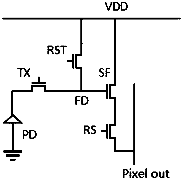
[0025] The content of the present invention will be described in detail below according to each accompanying drawing of the present invention. figure 1 It is an image sensor pixel circuit with a 4T structure in the prior art. As shown in the figure, the transfer transistor TX transfers the charge generated by the photoelectric effect of the photodiode PD to the floating diffusion region FD, and the gate of the source follower transistor SF is connected to The floating diffusion region FD amplifies the voltage signal of the floating diffusion region FD and outputs it to the column line (pixel out), and the reset transistor RST resets the voltage of the floating diffusion region FD according to the reset control signal.

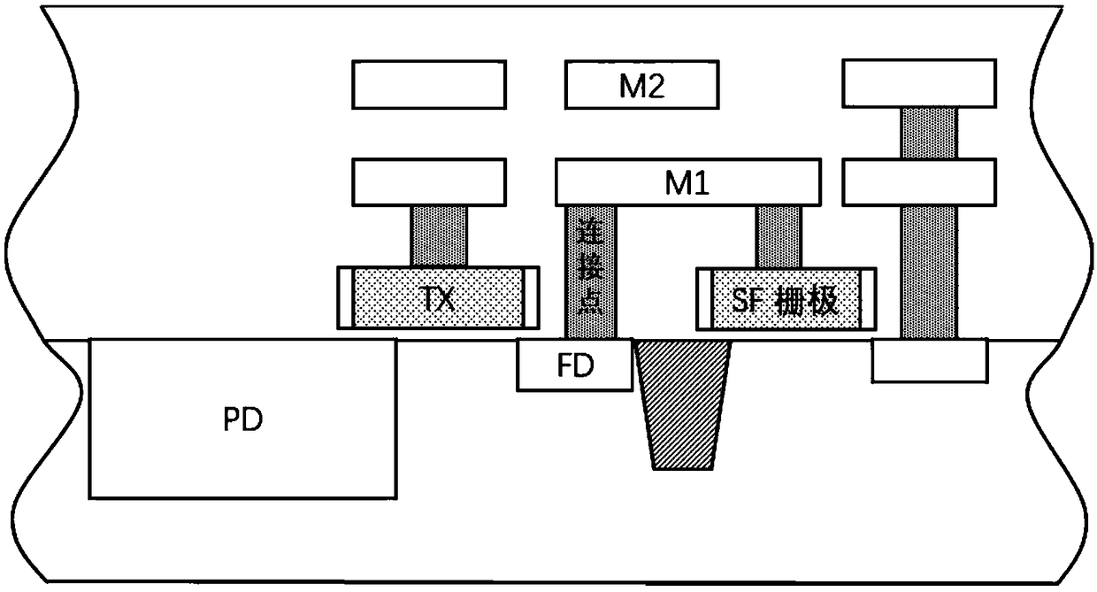
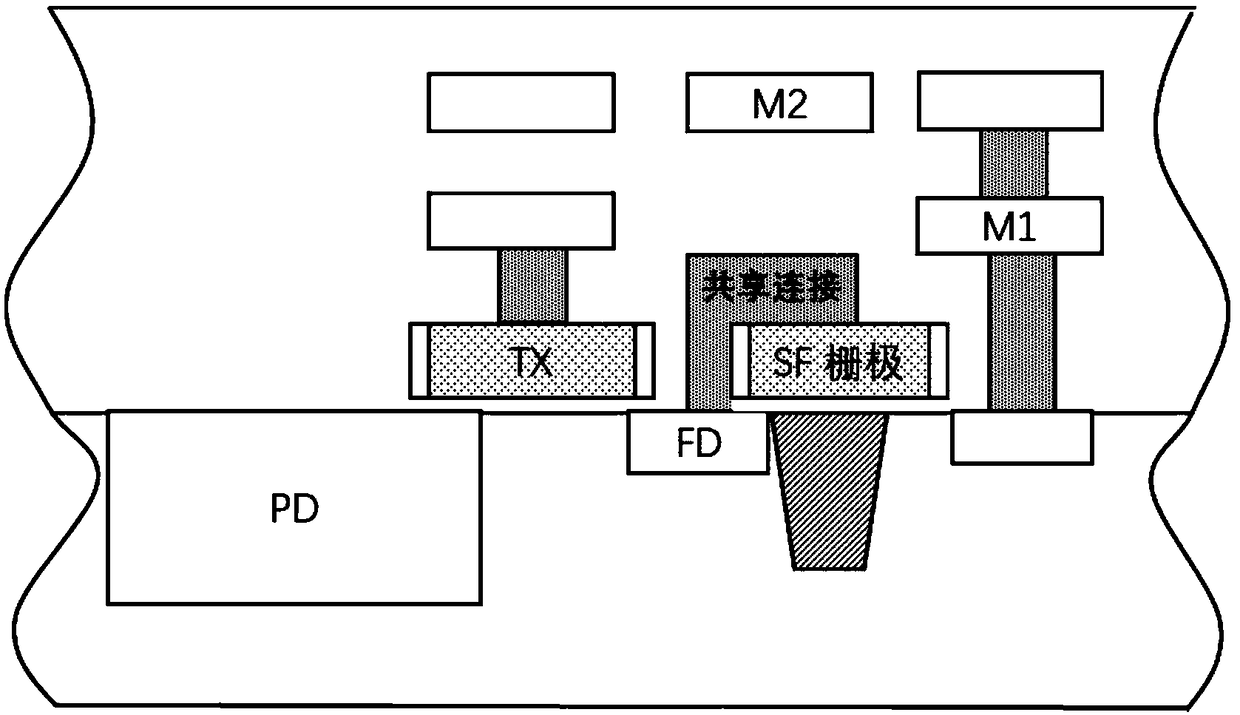
[0026] figure 2 is a cross-sectional schematic diagram of the connection between the floating diffusion region FD and the gate of the source follower transistor SF in an existing image sensor device. As shown in the figure, the floating diffusion region FD an...


PUM


Abstract

The invention provides an image sensor. The image sensor is provided with a plurality of pixel units which are formed on a semiconductor substrate and arranged in rows and columns, and each pixel unitcomprises one or more photodiodes, one or more of pass transistors, a reset transistor, and a source following transistor; the pass transistors are respectively connected to the respective photodiodes, and are used for transferring electric signals to a floating diffusion region; the reset transistor is connected to the floating diffusion region; and the grid of the source following transistor isconnected to the floating diffusion region to amplify and output the electric signal of the floating diffusion region. One part of the floating diffusion region is covered by one end of the grid of the source following transistor, so that a superposed region is formed; and a point of junction is shared by the grid of the source following transistor and the floating diffusion region, so that electric connection is formed. The image sensor proposed by the invention can effectively reduce the capacitance of the floating diffusion region, increase the conversion gain of a pixel circuit and reduceimage noise.

Description

technical field [0001] The invention relates to the technical field of image sensors, in particular to an image sensor design for realizing high conversion gain and low noise. Background technique [0002] CMOS image sensors are used in various fields. With the development and progress of technology, image sensor chips with lower power consumption, high integration and smaller size are the direction of application development. In various application fields, such as smartphones, micro-surveillance devices, digital cameras, etc., sensor chips for image output are increasingly miniaturized. In the process of image sensor design, manufacture and processing, in order to reduce the cost and chip design area, it is necessary to consider the circuit optimization design to reduce the image noise of the pixel circuit. [0003] In the pixel circuit design of an image sensor, a photodiode is usually used to convert the optical signal containing image information into an electrical sign...

Claims


Application Information

Patent Timeline
Patent Type & Authority Applications(China)
IPC IPC(8): H04N5/369H01L27/146
CPCH01L27/14612H04N25/70
Inventor 戚德奎石文杰
Owner 思特威(上海)电子科技股份有限公司
Why Eureka
Try Eureka