Forming method of touch display panel and touch display mother board

A technology of touch display panel and touch display, applied in the formation of touch display panel and the field of touch display motherboard, which can solve the misjudgment of display device detection of blue film, affect the quality of display device, affect the product yield, etc. problems, to achieve the effect of simple operation, improved stripping yield, and easy operation

Pending Publication Date: 2018-09-11
BOE TECH GRP CO LTD +1
View PDF7 Cites 2 Cited by
  • Summary
  • Abstract
  • Description
  • Claims
  • Application Information

AI Technical Summary

Problems solved by technology

[0003] However, there are still some problems in the manufacturing process of the touch display panel. After the touch sensor (TouchSensor) is manufactured, in order to protect the touch sensor from corrosion and wear in the subsequent process, a protective film is usually coated. Usually use screen printing screen to make a layer of blue film, when the blue film is removed, there will be residual phenomenon, which will seriously affect the quality of display devices
[0004] In addition, the display device with blue film may occasionally be misjudged during detection, which affects the yield of the product. Therefore, a new method of forming a touch display panel is needed to solve the above problems

Method used


Image

  • Forming method of touch display panel and touch display mother board
  • Forming method of touch display panel and touch display mother board
  • Forming method of touch display panel and touch display mother board

Examples


Embodiment Construction

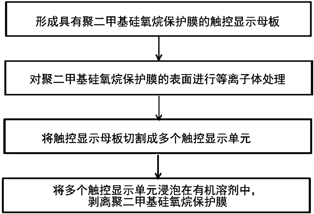
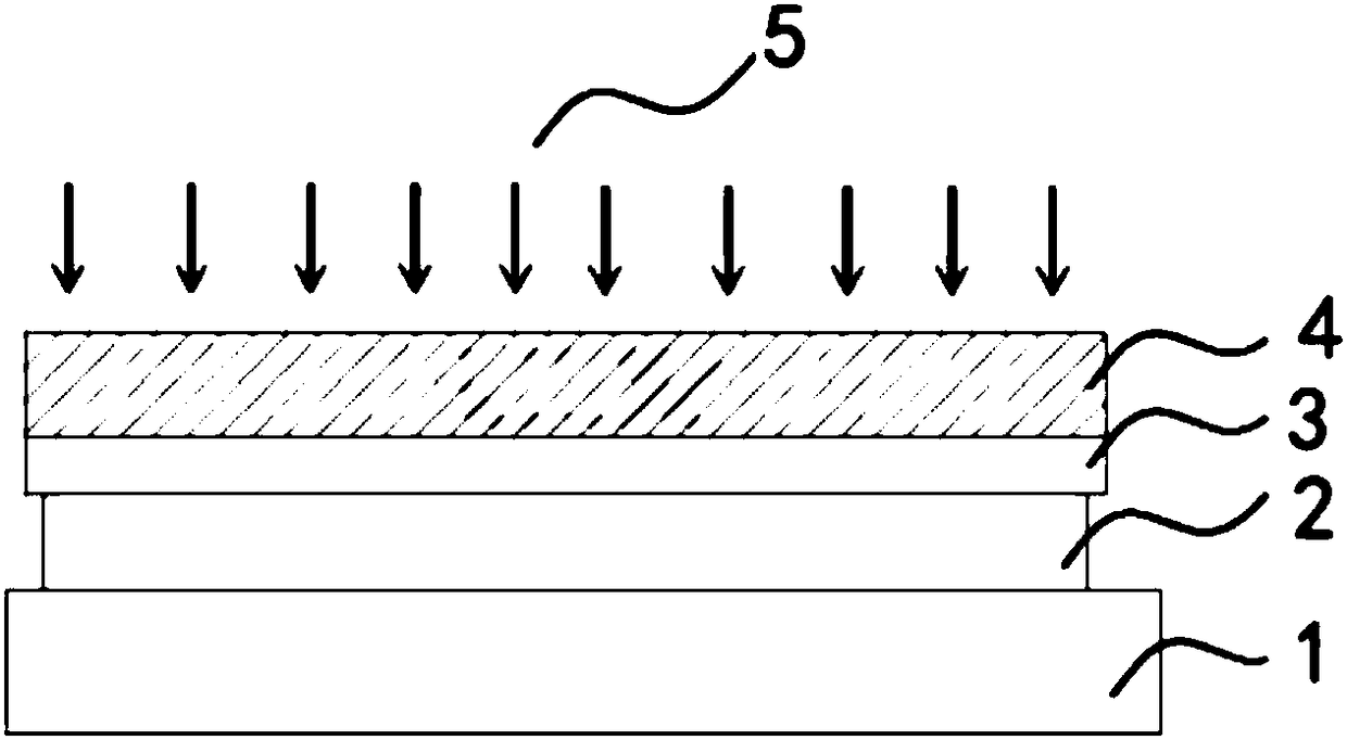
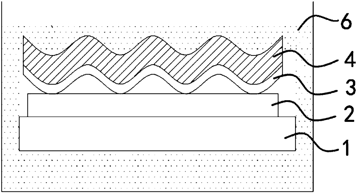
[0042] The implementation of the present invention is described below through specific specific examples, and those skilled in the art can easily understand the advantages and effects of the present invention from the content disclosed in this specification. The present invention can also be implemented or applied through other different implementation modes. The details in this specification can also be modified and changed based on different viewpoints and applications without departing from the concept disclosed in the present invention. Additionally, all ranges and values ​​herein are inclusive and combinable. Any numerical value or point, such as any integer, falling within the ranges stated herein can be used as minimum or maximum values ​​to derive lower ranges and the like.

[0043] It should be understood that the drawings disclosed herein are not necessarily shown in proportion to actual devices and components. The shapes and thicknesses of the embodiments may be ex...


PUM


Abstract

The invention provides a forming method of a touch display panel and a touch display mother board. The forming method of the touch display panel comprises the steps that the touch display mother boardwith a polydimethylsiloxane protection film is formed, and the surface of the polydimethylsiloxane protection film is subjected to plasma treatment; the touch display mother board is cut into a plurality of touch display units; the touch display units are soaked in an organic solvent, and the polydimethylsiloxane protection film is stripped off. Polydimethylsiloxane subjected to plasma treatmentis adopted as a protection film of a touch sensor in the manufacturing process; the touch display units are soaked in the organic solvent in the stripping-off process, and therefore the adhesivity between the protection film and the touch sensor is reduced, so that the protection film is easy to strip off and free of residues, operation is easy, and the stripping-off yield is remarkably increased.

Description

technical field [0001] The invention relates to the technical field of liquid crystal display, in particular to a method for forming a touch display panel and a touch display motherboard. Background technique [0002] With the development of science and technology, liquid crystal displays can be seen everywhere in life. In order to improve the operational sense of human-computer interaction, touch display panels are widely used, such as mobile phones, tablet computers, and bank self-service all-in-one machines. [0003] However, there are still some problems in the manufacturing process of the touch display panel. After the touch sensor (TouchSensor) is manufactured, in order to protect the touch sensor from corrosion and wear in the subsequent process, a protective film is usually coated. Usually a layer of blue film is made with a screen printing screen. When the blue film is removed, there will be residues, which will seriously affect the quality of the display device. ...

Claims


Application Information

Patent Timeline
IPC IPC(8): G06F3/041G02F1/1333
CPCG02F1/1333G02F1/13338G06F3/0412G06F2203/04103
Inventor 吴小会姜妮向西冯远明
Owner BOE TECH GRP CO LTD
Why Eureka
Try Eureka