Semiconductor structure and formation method thereof

A technology of semiconductor and hole structure, applied in the field of semiconductor structure and its formation, can solve the problems such as the decrease of product reliability, the influence of the current transmission effect on the surface of the semiconductor layer, and the influence of the product yield rate, etc. The effect of defects

Pending Publication Date: 2018-09-14
YANGTZE MEMORY TECH CO LTD
View PDF12 Cites 24 Cited by
  • Summary
  • Abstract
  • Description
  • Claims
  • Application Information

AI Technical Summary

Problems solved by technology

[0003] In order to further increase the bit density of the 3D NAND flash memory structure, a double-layer or multi-layer channel hole structure is applied, and a semiconductor layer between the upper and lower channel hole structures, such as a polysilicon layer, is used between the multi-layer channel hole structures. , to carry out current transmission, and the surface of the semiconductor layer is prone to defects when etching the upper channel hole, which will affect the current transmission effect on the surface of the semiconductor layer, thereby affecting the yield of the product and resulting in a decrease in the reliability of the product

Method used


Image

  • Semiconductor structure and formation method thereof
  • Semiconductor structure and formation method thereof
  • Semiconductor structure and formation method thereof

Examples


Embodiment Construction

[0025] Specific implementations of the semiconductor structure and its forming method provided by the present invention will be described in detail below in conjunction with the accompanying drawings.

[0026] Please refer to Figure 1 to Figure 8 , is a structural schematic diagram of the formation process of the semiconductor structure according to a specific embodiment of the present invention.

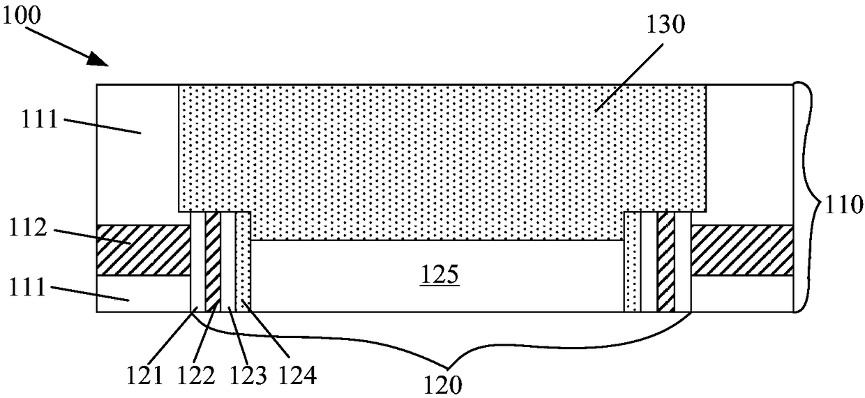
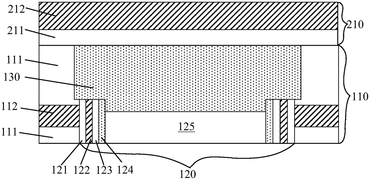
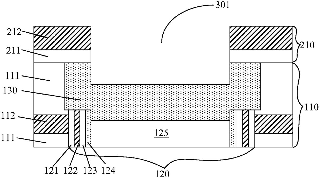
[0027] Please refer to figure 1 A substrate 100 is provided, the substrate 100 includes a first stack structure 110 , a first channel hole structure 120 penetrating through the first stack structure 110 , and a semiconductor layer 130 is formed on the top of the first channel hole structure 120 .

[0028] The base 100 includes a substrate (not shown in the figure), forming a first stacked structure 110 stacked with the surface of the substrate along a direction perpendicular to the surface of the substrate, and the first stacked structure 110 includes first insulating layer 111 a...


PUM


Abstract

The present invention relates to a semiconductor structure and a formation method thereof. The formation method of the semiconductor structure comprises the steps of: providing a substrate, wherein the substrate comprises a first stacked structure and a first channel hole structure penetrating the first stacked structure, wherein the top portion of the first channel hole structure is provided witha semiconductor layer; forming a second stacked structure at the surface of the substrate; forming a second channel hole configured to penetrate the second stacked structure and the semiconductor layer with partial depth; performing oxidation processing of the surface of the semiconductor layer at the bottom portion of the second channel hole to form an oxidation layer; forming a function layer covering the inner wall of the second channel hole; removing the function layer and the oxidation layer located at the bottom portion of the second channel hole to form a second function layer, and exposing the semiconductor layer under the oxidation layer; and forming a second channel layer at the surface of the second function layer and the surface of the exposed semiconductor layer. The formation method can improve the quality of the semiconductor layer so as to improve the performances of the semiconductor structure.

Description

technical field [0001] The invention relates to the technical field of semiconductors, in particular to a semiconductor structure and a forming method thereof. Background technique [0002] In recent years, the development of flash memory (Flash Memory) is particularly rapid. The main feature of flash memory is that it can keep stored information for a long time without power on, and has the advantages of high integration, fast access speed, easy erasing and rewriting, etc. Has been widely used. In order to further increase the bit density (Bit Density) of the flash memory while reducing the bit cost (Bit Cost), three-dimensional flash memory (3D NAND) technology has been developed rapidly. [0003] In order to further increase the bit density of the 3D NAND flash memory structure, a double-layer or multi-layer channel hole structure is applied, and a semiconductor layer between the upper and lower channel hole structures, such as a polysilicon layer, is used between the m...

Claims


Application Information

Patent Timeline
Patent Type & Authority Applications(China)
IPC IPC(8): H01L27/1157H01L27/115
CPCH10B43/35H10B69/00
Inventor 杨号号王恩博张勇陶谦胡禺石吕震宇卢峰
Owner YANGTZE MEMORY TECH CO LTD
Why Eureka
Try Eureka