Display substrate, manufacturing method thereof and display device

A technology for display substrates and substrate substrates, applied in organic semiconductor devices, optics, instruments, etc., can solve the problems of increasing the thickness of the passivation layer and reducing the storage capacitance, avoiding the influence of the capacitance and ensuring the compression performance. , to ensure the effect of the display effect

Active Publication Date: 2018-09-18
BOE TECH GRP CO LTD
View PDF7 Cites 13 Cited by
  • Summary
  • Abstract
  • Description
  • Claims
  • Application Information

AI Technical Summary

Problems solved by technology

[0005] The invention provides a display substrate, a manufacturing method thereof, and a display device, which can solve the problem in the related art that the capacity of the storage capacitor decreases due to the increase in the thickness of the passivation layer

Method used


Image

  • Display substrate, manufacturing method thereof and display device
  • Display substrate, manufacturing method thereof and display device
  • Display substrate, manufacturing method thereof and display device

Examples


Embodiment Construction

[0050] In order to make the objectives, technical solutions, and advantages of the present invention clearer, the embodiments of the present invention will be described in further detail below in conjunction with the accompanying drawings.

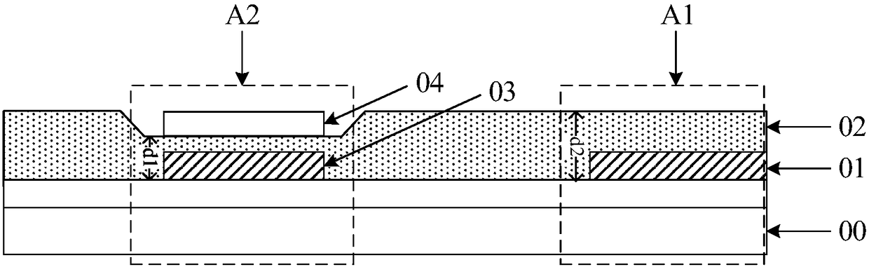
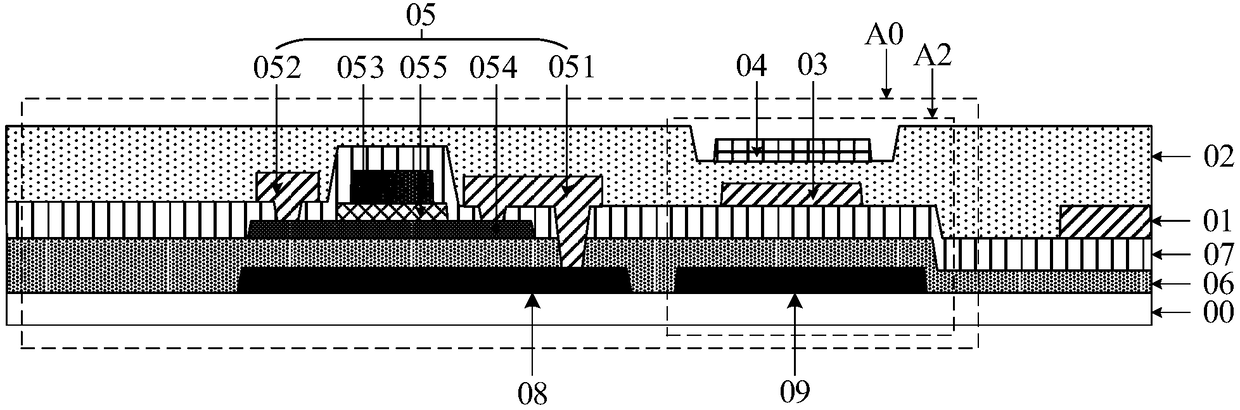
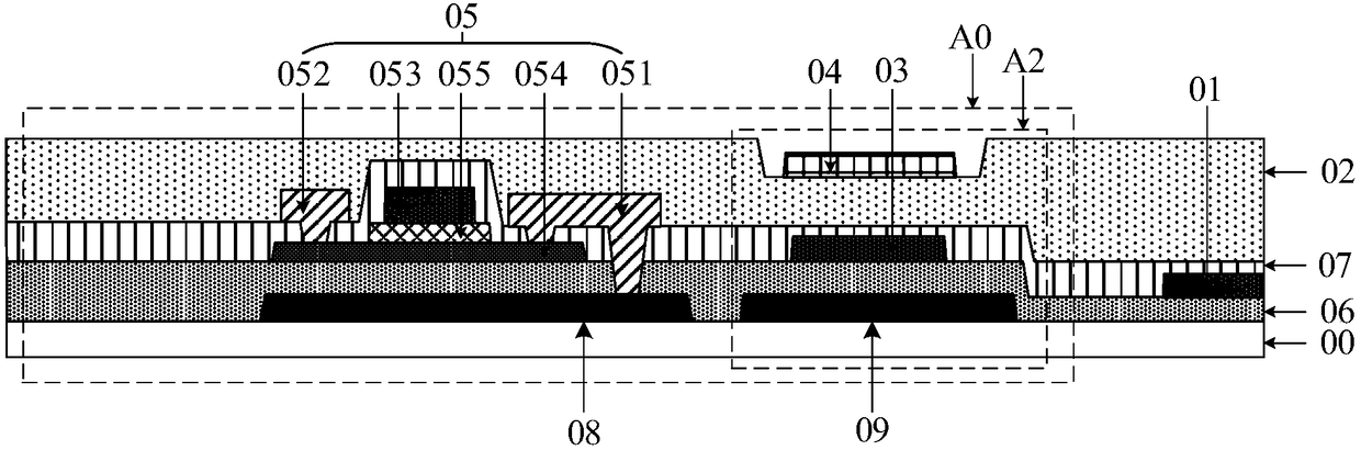
[0051] figure 1 Is a schematic structural diagram of a display substrate provided by an embodiment of the present invention, such as figure 1 As shown, the display substrate may include:

[0052] The base substrate 00, the metal layer 01 disposed in the peripheral area A1 of the base substrate 00, and the passivation layer 02 disposed on the side of the metal layer 01 away from the base substrate 00 and covering the base substrate 00.

[0053] In the capacitor area A2 of the base substrate 00, capacitor electrodes 03 and 04 are respectively provided on both sides of the passivation layer 02. The capacitor electrodes 03 and 04 on both sides of the passivation layer 02 can form a storage capacitor in the display substrate. The storage capacitor ca...


PUM

PropertyMeasurementUnit
thicknessaaaaaaaaaa
thicknessaaaaaaaaaa
thicknessaaaaaaaaaa

Abstract

The invention provides a display substrate, a manufacturing method thereof and a display device, and relates to the technical field of display. The display substrate comprises a substrate base plate,a metal layer arranged in the periphery region of the substrate base plate, and a passivation layer which is arranged on one side, away from the substrate base plate, of the metal layer and covers thesubstrate base plate. In the capacitance region of the substrate base plate, capacitance electrodes are arranged on two sides of the passivation layer. The thickness of the passivation layer in the capacitance region is smaller than the thickness of the passivation layer in the periphery region. According to the invention, the passivation layer in the display substrate is partially quite thick inthe periphery region; the anti-compression performance is quite good; the passivation region is quite thin in the capacitance region; capacity of the storage capacitance will not be affected; and display effects of the display device are ensured.

Description

Technical field [0001] The present invention relates to the field of display technology, in particular to a display substrate, a manufacturing method thereof, and a display device. Background technique [0002] After the display substrate is manufactured, the signal lines on the display substrate and the drive circuit need to be bonded, that is, the signal lines and the drive circuit need to be pressed and connected. However, during the bonding process, the passivation layer in the peripheral area of ​​the display substrate may be crushed, causing the metal layer of the passivation layer close to the base substrate to be exposed to water and oxygen, and the metal layer is prone to corrosion and fracture. . [0003] In the related art, in order to prevent the passivation layer located in the peripheral area from being crushed during the bonding process, the thickness of the passivation layer formed in the display substrate is generally increased to increase the pressure resistance ...

Claims


Application Information

Patent Timeline
Patent Type & Authority Applications(China)
IPC IPC(8): H01L27/12G02F1/1333
CPCH01L27/1214H01L27/1259G02F1/1333H01L27/1255H01L29/78633H01L29/7869H10K59/124H10K59/1216H10K59/126H10K59/131H10K59/1201H10K2102/351H10K50/818H10K59/38H10K71/00
Inventor 方金钢成军赵策丁录科刘宁
Owner BOE TECH GRP CO LTD
Why Eureka
Try Eureka