Semiconductor chip overflow material quick detection method based on image segmentation algorithm

A technology of image segmentation and detection methods, applied in image analysis, image enhancement, image data processing, etc.

Active Publication Date: 2018-09-28
ZHEJIANG UNIV
View PDF3 Cites 6 Cited by
  • Summary
  • Abstract
  • Description
  • Claims
  • Application Information

AI Technical Summary

Problems solved by technology

[0005] The purpose of the present invention is to provide a fast flash detec...

Method used


Image

  • Semiconductor chip overflow material quick detection method based on image segmentation algorithm
  • Semiconductor chip overflow material quick detection method based on image segmentation algorithm
  • Semiconductor chip overflow material quick detection method based on image segmentation algorithm

Examples


Embodiment Construction

[0063] The present invention will be described in further detail below in conjunction with the accompanying drawings and specific examples.

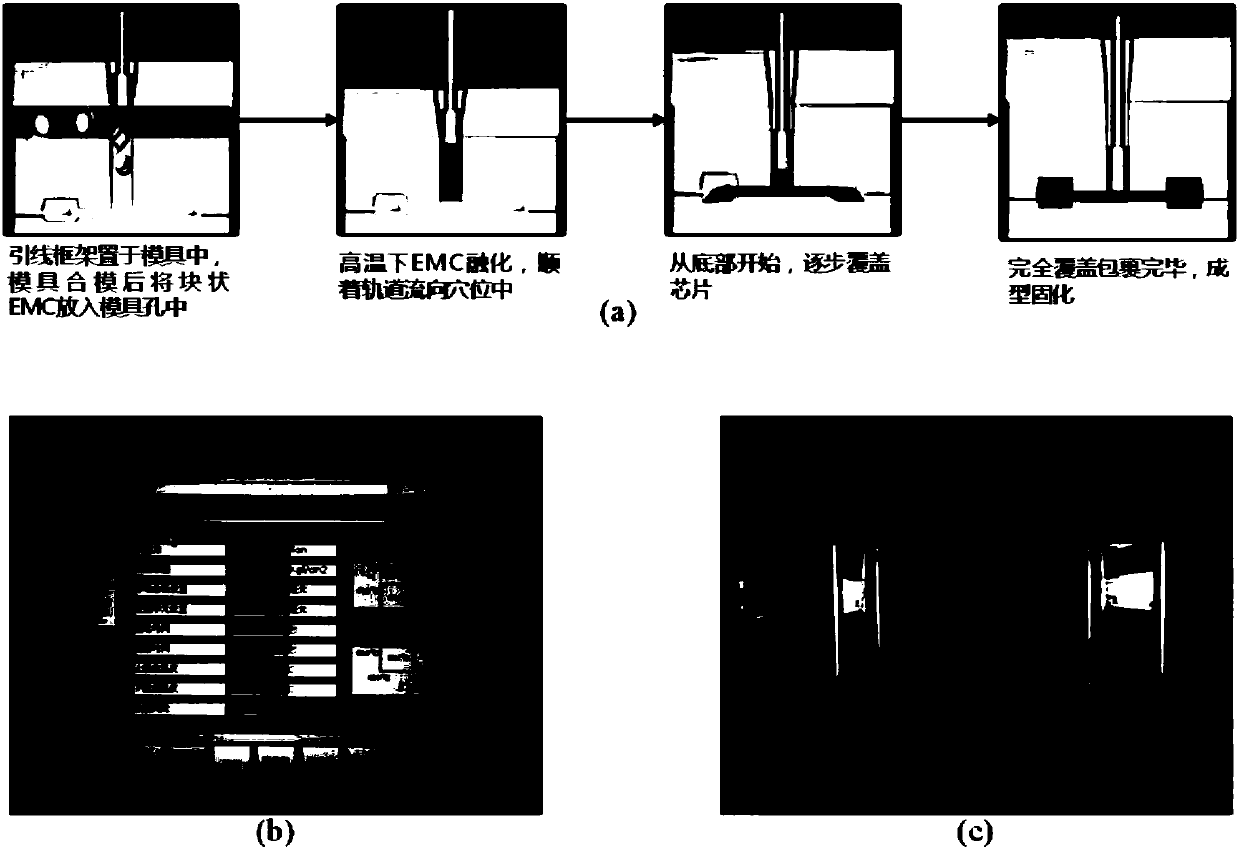
[0064] (1) EMC (Epoxy molding compound) packaging: such as figure 1 As shown in (a), the lead frame is placed in the mold so that each chip is located in the hole, and the block EMC is placed in the mold space after the mold is closed. according to figure 1 (b) Set the parameters of the packaging press as shown in (b). At high temperature, the EMC begins to melt, and flows along the track to the acupuncture points, gradually covering the chip from the bottom until it is completely covered and wrapped, and then molded and solidified, as shown in figure 1 as shown in (c);

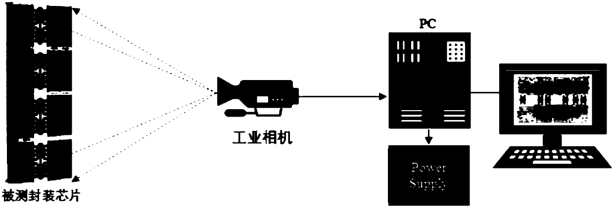
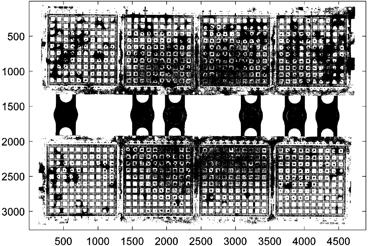
[0065] (2) Image acquisition and preprocessing: image-based flash detection systems such as figure 2 As shown, the use of industrial cameras to obtain such as image 3 The grayscale image of the original packaging film shown has a resolution of 3264*4896. Through G...


PUM


Abstract

The invention discloses a semiconductor chip overflow material quick detection method based on an image segmentation algorithm. The method aims to provide timely feedback information for an EMC (EpoxyMolding Compound) encapsulation process by recognizing redundancy overflowing to pins and an exposed carrier in the integrated circuit EMC encapsulation process. According to the method, first, an original chip image obtained after EMC encapsulation formation and collected by an industrial camera is preprocessed; next, a selective search algorithm is utilized to perform image segmentation to obtain target candidate regions, and a to-be-detected chip region is screened out of the target candidate regions; and then threshold segmentation is performed on the screened region to obtain an overflowmaterial region. Through the method, an overflow material detection result of each chip can be given in an extremely short time, the overflow material detection means in the EMC encapsulation processare optimized, the real-time feedback information is provided for the EMC encapsulation process, and therefore EMC encapsulation performance is improved.

Description

technical field [0001] The invention belongs to the field of integrated circuit EMC packaging overflow detection, in particular to a method for quickly detecting semiconductor chip overflow based on an image segmentation algorithm. Background technique [0002] EMC is an important microelectronic packaging material. Through the packaging process, the semiconductor chip is covered to form a protection, so as not to be damaged by the external environment. At the same time, EMC also has a certain heat dissipation effect. EMC has the characteristics of large-scale production and reasonable reliability. It is one of the common packaging materials for semiconductor packaging and occupies more than 95% of the packaging market with its unique advantages. However, in the semiconductor plastic packaging process, due to the gap between the lead frame and the plastic packaging film, the gel-like plastic packaging material will leak out from the gap, solidify on the surface of the lead b...

Claims


Application Information

Patent Timeline
IPC IPC(8): G06T7/00G06T7/11G06T7/136G06T7/90G06T7/44
CPCG06T7/0004G06T7/11G06T7/136G06T7/44G06T7/90G06T2207/10024G06T2207/30148
Inventor 赵春晖王晶
Owner ZHEJIANG UNIV
Why Eureka
Try Eureka